

Key Insights
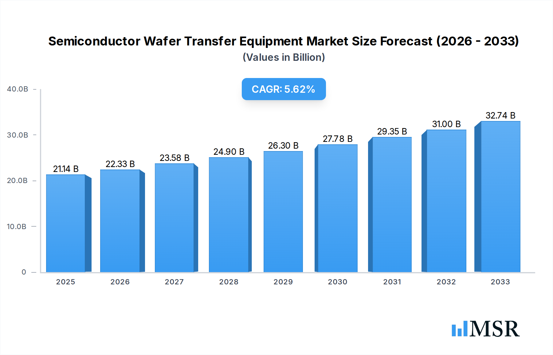
The global Semiconductor Wafer Transfer Equipment market is poised for robust growth, projected to reach USD 21,140 million by 2025, with a Compound Annual Growth Rate (CAGR) of 5.7% during the forecast period of 2025-2033. This expansion is primarily driven by the escalating demand for advanced semiconductor devices across various industries, including consumer electronics, automotive, and telecommunications. The increasing complexity of wafer fabrication processes, coupled with the need for higher throughput and enhanced yield, necessitates sophisticated wafer transfer solutions. The market is witnessing a significant surge in the adoption of 300 mm wafer transfer equipment, reflecting the industry's shift towards larger wafer diameters to improve manufacturing efficiency and reduce costs. Furthermore, the growing investment in research and development for next-generation semiconductor technologies, such as artificial intelligence and 5G, is a key propellant for market expansion. Innovations in monolithic transfer equipment, offering greater precision and automation, are also contributing to the market's upward trajectory.

Semiconductor Wafer Transfer Equipment Market Size (In Billion)
The market's growth is further bolstered by trends such as the miniaturization of electronic components and the rising adoption of automation in manufacturing facilities. Enhanced precision, contamination control, and speed are paramount in semiconductor manufacturing, directly influencing the demand for advanced wafer transfer systems. Regions like Asia Pacific, particularly China, Japan, and South Korea, are expected to lead the market share due to their established semiconductor manufacturing hubs and continuous investments in expanding production capacities. However, the market may face certain restraints, including the high initial investment costs for advanced transfer equipment and the fluctuating geopolitical landscape that can impact global supply chains and trade dynamics. Despite these challenges, the relentless pursuit of technological advancements and the ever-increasing global demand for semiconductors are set to sustain the positive growth momentum of the Semiconductor Wafer Transfer Equipment market.
Semiconductor Wafer Transfer Equipment Company Market Share
Here is an SEO-optimized and engaging report description for Semiconductor Wafer Transfer Equipment, incorporating all your specified details.
Semiconductor Wafer Transfer Equipment Market Concentration & Dynamics
The semiconductor wafer transfer equipment market exhibits a moderate to high concentration, with key players like RORZE Corporation, DAIHEN Corporation, Hirata Corporation, Sinfonia Technology, Nidec (Genmark Automation), JEL Corporation, Cymechs Inc, Robostar, Robots and Design (RND), RAONTEC Inc, KORO, Brooks Automation, Quartet Mechanics, Milara Inc., RECIF Technologies, Sanwa Engineering, HIWIN TECHNOLOGIES, Siasun Robot & Automation, Beijing U-PRECISION TECH, Beijing Jingyi Automation, Shanghai Guona, Shanghai Fortrend, and Shanghai MICSON holding significant market shares. The innovation ecosystem is driven by continuous advancements in automation, precision, and throughput, essential for handling increasingly complex semiconductor devices. Regulatory frameworks, primarily focused on safety and environmental standards, play a role in market entry and product development, although direct governmental intervention is minimal. Substitute products, such as manual handling systems (though largely obsolete for advanced nodes), are not a significant threat due to the critical need for contamination control and precision. End-user trends, including the demand for higher yields, reduced defect rates, and the transition to larger wafer diameters (300 mm Wafer), are shaping the product development strategies of equipment manufacturers. Mergers and Acquisition (M&A) activities, while not as frequent as in some other sectors, are strategically important for companies seeking to expand their product portfolios, technological capabilities, or geographic reach. The number of M&A deals in the historical period (2019-2024) is estimated to be in the low tens, primarily involving smaller technology firms being acquired by larger players to enhance their automation and robotics offerings.
Semiconductor Wafer Transfer Equipment Industry Insights & Trends
The global Semiconductor Wafer Transfer Equipment market is poised for substantial growth, projected to expand from an estimated market size of $X.XX million in the base year of 2025 to $Y.YY million by the end of the forecast period in 2033, exhibiting a Compound Annual Growth Rate (CAGR) of Z.ZZ%. This robust expansion is underpinned by several critical industry developments and accelerating trends. The insatiable global demand for advanced semiconductor devices across a multitude of applications, including consumer electronics, automotive, AI, and telecommunications, forms the bedrock of this market's ascent. As chip complexity increases and manufacturing processes become more sophisticated, the need for highly precise, reliable, and automated wafer transfer solutions becomes paramount. This directly fuels the demand for cutting-edge equipment capable of handling delicate wafers with utmost care, minimizing particulate contamination and ensuring optimal yield.
Technological disruptions are a constant feature, with significant investment flowing into research and development. Innovations in robotics, artificial intelligence (AI) for process optimization, advanced sensor technologies for defect detection, and improved material handling techniques are continuously pushing the boundaries of wafer transfer capabilities. The industry is witnessing a strong push towards higher throughput and greater flexibility in transfer systems, catering to the diverse needs of both 200 mm Wafer and 300 mm Wafer manufacturing lines. Furthermore, the increasing adoption of Industry 4.0 principles, including the integration of smart factory concepts, data analytics for predictive maintenance, and enhanced connectivity, is transforming how wafer transfer equipment is designed, operated, and maintained. Evolving consumer behaviors, while indirectly influencing this market, are indirectly driving innovation through the demand for smaller, more powerful, and energy-efficient electronic devices, which in turn necessitate advanced semiconductor manufacturing. The strategic shift towards onshoring and nearshoring semiconductor manufacturing by various governments globally is also a significant growth catalyst, leading to increased capital expenditure in fabrication facilities and, consequently, in sophisticated wafer transfer equipment. The historical period of 2019–2024 saw steady growth, laying a strong foundation for the projected acceleration in the forecast period.
Key Markets & Segments Leading Semiconductor Wafer Transfer Equipment
The 300 mm Wafer segment is a primary driver of growth in the Semiconductor Wafer Transfer Equipment market, demonstrating significant dominance throughout the study period (2019–2033). This ascendancy is propelled by the global industry's strategic focus on advanced node manufacturing, where larger wafer diameters are essential for achieving economies of scale and reducing the cost per chip. The economic growth experienced in key semiconductor manufacturing hubs worldwide, coupled with substantial government incentives and investments in building state-of-the-art fabrication plants, has directly translated into increased demand for high-capacity and highly automated wafer transfer solutions for 300 mm lines.
- Drivers for 300 mm Wafer Dominance:
- Economies of Scale: Larger wafer sizes allow for the production of more chips per wafer, significantly reducing manufacturing costs.
- Technological Advancements: The development of advanced semiconductor nodes (e.g., 7nm, 5nm, 3nm) is predominantly carried out on 300 mm wafers, necessitating specialized transfer equipment.
- Infrastructure Investment: Major semiconductor manufacturers are investing billions of dollars in new and expanded 300 mm fabs, creating a substantial market for related equipment.
- Yield Improvement Focus: The precision and automation offered by modern wafer transfer equipment are crucial for maximizing yield on expensive 300 mm wafers.
Geographically, Asia-Pacific, particularly countries like Taiwan, South Korea, and China, stands as the leading region for Semiconductor Wafer Transfer Equipment consumption and innovation. This is driven by the presence of major foundries and integrated device manufacturers (IDMs) within these regions. The robust growth in demand for consumer electronics, automotive semiconductors, and high-performance computing components manufactured in this region directly fuels the need for advanced wafer handling systems. The rapid expansion of semiconductor manufacturing capacity in China, supported by national strategic initiatives, further solidifies Asia-Pacific's leading position.
The Monolithic Transfer Equipment type is also experiencing significant traction due to its inherent advantages in terms of precision, cleanliness, and speed, particularly for high-volume, sensitive manufacturing processes. While Batch Transfer Equipment continues to be relevant for specific applications or older node technologies, the industry's trajectory clearly favors the advanced capabilities offered by monolithic solutions.
Semiconductor Wafer Transfer Equipment Product Developments
Product innovations in Semiconductor Wafer Transfer Equipment are intensely focused on enhancing precision, throughput, and contamination control. Manufacturers are developing next-generation systems incorporating advanced robotics, AI-driven path optimization, and improved sensor technologies for real-time defect detection. The integration of vacuum-compatible components, hermetically sealed transfer pathways, and advanced cleanroom designs are crucial for handling sensitive next-generation semiconductor materials and devices. Furthermore, the increasing demand for flexible and modular transfer solutions that can adapt to evolving fab layouts and production needs is driving significant R&D efforts, offering competitive edges to companies that can deliver highly reliable and efficient systems for both 200 mm Wafer and 300 mm Wafer applications.
Challenges in the Semiconductor Wafer Transfer Equipment Market
The Semiconductor Wafer Transfer Equipment market faces several critical challenges that could impede its growth trajectory. High initial capital investment for advanced equipment represents a significant barrier for smaller fabs or those with budget constraints. The stringent quality and contamination control requirements necessitate meticulous design, manufacturing, and maintenance, leading to higher operational costs. Supply chain disruptions, particularly for specialized components and raw materials, can lead to production delays and increased lead times, impacting the overall availability of critical equipment. Intense competition among established players and emerging technologies also puts pressure on pricing and profitability, requiring continuous innovation to maintain market share.
Forces Driving Semiconductor Wafer Transfer Equipment Growth
Several powerful forces are propelling the growth of the Semiconductor Wafer Transfer Equipment market. The relentless global demand for advanced semiconductors, driven by burgeoning applications in AI, 5G, autonomous vehicles, and the Internet of Things (IoT), is the primary catalyst. Technological advancements in semiconductor manufacturing, including the transition to smaller process nodes and novel materials, necessitate increasingly sophisticated and precise wafer handling solutions. Government initiatives worldwide aimed at bolstering domestic semiconductor manufacturing capabilities, coupled with substantial investments in R&D and fab construction, are creating unprecedented market opportunities. Furthermore, the industry's ongoing pursuit of higher manufacturing yields, reduced defect rates, and improved operational efficiency directly fuels the adoption of advanced automated wafer transfer systems.
Challenges in the Semiconductor Wafer Transfer Equipment Market
Long-term growth catalysts in the Semiconductor Wafer Transfer Equipment market are intrinsically linked to continued technological innovation and strategic market expansion. The industry's ability to develop increasingly intelligent and adaptive transfer systems, capable of handling next-generation wafer sizes and complex 3D architectures, will be crucial. Strategic partnerships and collaborations between equipment manufacturers, semiconductor device developers, and research institutions will foster accelerated innovation and problem-solving. Furthermore, the expansion of semiconductor manufacturing into new geographical regions and the development of specialized transfer solutions for emerging applications, such as advanced packaging and MEMS fabrication, present significant long-term growth avenues.
Emerging Opportunities in Semiconductor Wafer Transfer Equipment
Emerging opportunities in the Semiconductor Wafer Transfer Equipment market are ripe for exploitation, driven by evolving industry needs and technological advancements. The increasing focus on advanced packaging techniques, such as fan-out wafer-level packaging, presents a unique demand for specialized wafer handling solutions. The growing adoption of AI and machine learning in semiconductor manufacturing is creating opportunities for smarter, self-optimizing wafer transfer systems that can predict and prevent potential issues. Furthermore, the development of sustainable and energy-efficient wafer transfer equipment aligns with global environmental initiatives, offering a competitive advantage. The growing demand for customized and modular transfer solutions that can be easily integrated into existing fab infrastructure is another significant emerging trend.
Leading Players in the Semiconductor Wafer Transfer Equipment Sector
- RORZE Corporation
- DAIHEN Corporation
- Hirata Corporation
- Sinfonia Technology
- Nidec (Genmark Automation)
- JEL Corporation
- Cymechs Inc
- Robostar
- Robots and Design (RND)
- RAONTEC Inc
- KORO
- Brooks Automation
- Quartet Mechanics
- Milara Inc.
- RECIF Technologies
- Sanwa Engineering
- HIWIN TECHNOLOGIES
- Siasun Robot & Automation
- Beijing U-PRECISION TECH
- Beijing Jingyi Automation
- Shanghai Guona
- Shanghai Fortrend
- Shanghai MICSON
Key Milestones in Semiconductor Wafer Transfer Equipment Industry
- 2019: Introduction of advanced AI-powered path planning algorithms for wafer robots, significantly improving transfer efficiency and reducing cycle times.
- 2020: Launch of new vacuum-compatible wafer handling systems designed for ultra-high vacuum environments, critical for advanced deposition processes.
- 2021: Significant increase in M&A activity as larger automation companies acquired niche robotic and handling technology firms to expand their semiconductor offerings.
- 2022: Development of enhanced contamination detection and prevention technologies integrated directly into wafer transfer equipment, leading to improved yields.
- 2023: Increased focus on modular and scalable wafer transfer solutions to accommodate evolving fab layouts and diverse production needs.
- 2024: Advancements in predictive maintenance capabilities for wafer transfer equipment, utilizing IoT sensors and data analytics to minimize downtime.
- 2025 (Estimated): Expectation of widespread adoption of ultra-clean wafer transfer technologies to support the manufacturing of next-generation semiconductor devices.
Strategic Outlook for Semiconductor Wafer Transfer Equipment Market
The strategic outlook for the Semiconductor Wafer Transfer Equipment market is overwhelmingly positive, characterized by sustained growth and innovation. Key accelerators will include the continued global expansion of semiconductor manufacturing, driven by both consumer demand and national strategic interests. Manufacturers that can offer highly integrated, intelligent, and customizable wafer transfer solutions will be best positioned to capitalize on this growth. Strategic investments in research and development focused on enabling advanced packaging technologies and supporting the transition to larger wafer sizes will be paramount. Furthermore, the increasing demand for automation and efficiency across the entire semiconductor manufacturing value chain will create ongoing opportunities for suppliers of cutting-edge wafer transfer equipment.
Semiconductor Wafer Transfer Equipment Segmentation
-
1. Application
- 1.1. 200 mm Wafer
- 1.2. 300 mm Wafer
- 1.3. Others
-
2. Types
- 2.1. Monolithic Transfer Equipment
- 2.2. Batch Transfer Equipment
Semiconductor Wafer Transfer Equipment Segmentation By Geography
-
1. North America
- 1.1. United States
- 1.2. Canada
- 1.3. Mexico
-
2. South America
- 2.1. Brazil
- 2.2. Argentina
- 2.3. Rest of South America
-
3. Europe
- 3.1. United Kingdom
- 3.2. Germany
- 3.3. France
- 3.4. Italy
- 3.5. Spain
- 3.6. Russia
- 3.7. Benelux
- 3.8. Nordics
- 3.9. Rest of Europe
-
4. Middle East & Africa
- 4.1. Turkey
- 4.2. Israel
- 4.3. GCC
- 4.4. North Africa
- 4.5. South Africa
- 4.6. Rest of Middle East & Africa
-
5. Asia Pacific
- 5.1. China
- 5.2. India
- 5.3. Japan
- 5.4. South Korea
- 5.5. ASEAN
- 5.6. Oceania
- 5.7. Rest of Asia Pacific
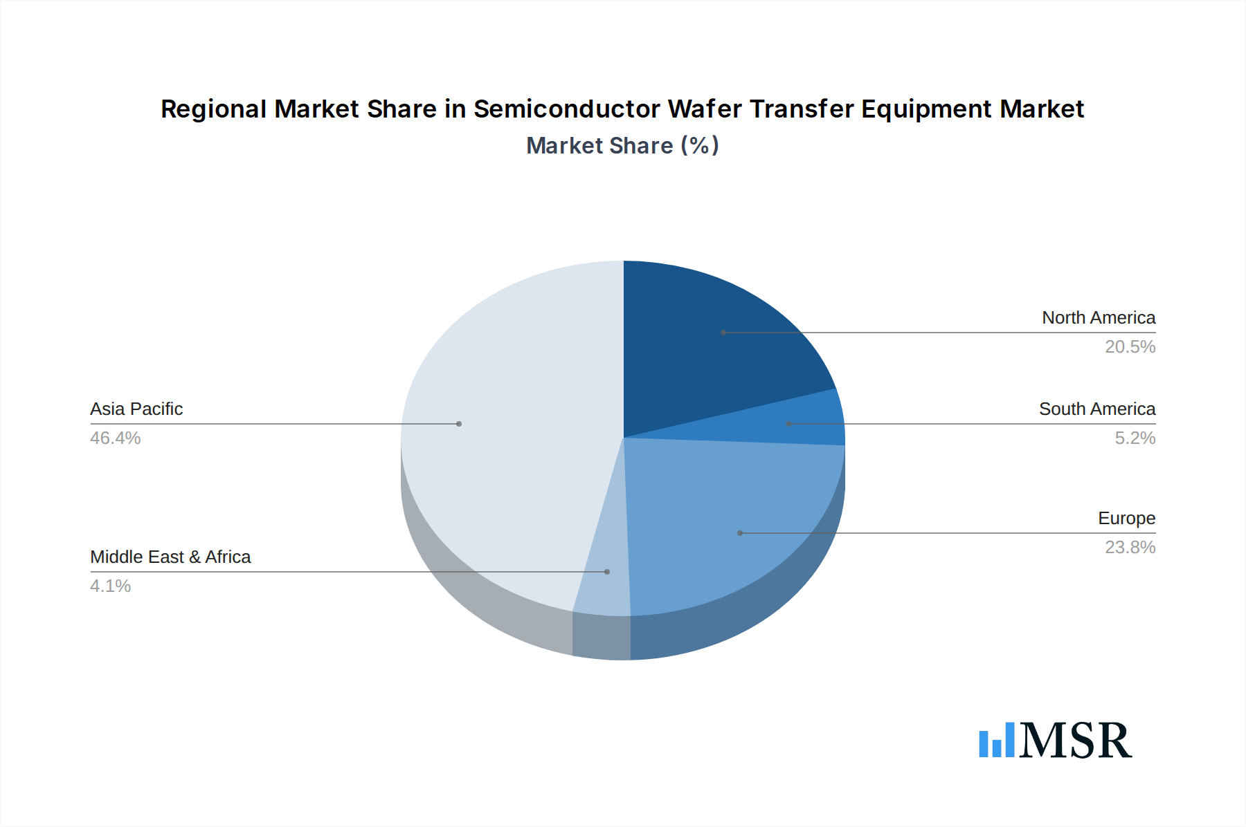
Semiconductor Wafer Transfer Equipment Regional Market Share
Geographic Coverage of Semiconductor Wafer Transfer Equipment
Semiconductor Wafer Transfer Equipment REPORT HIGHLIGHTS
| Aspects | Details |
|---|---|
| Study Period | 2020-2034 |
| Base Year | 2025 |
| Estimated Year | 2026 |
| Forecast Period | 2026-2034 |
| Historical Period | 2020-2025 |
| Growth Rate | CAGR of 5.7% from 2020-2034 |
| Segmentation |
|
Table of Contents
- 1. Introduction
- 1.1. Research Scope
- 1.2. Market Segmentation
- 1.3. Research Methodology
- 1.4. Definitions and Assumptions
- 2. Executive Summary
- 2.1. Introduction
- 3. Market Dynamics
- 3.1. Introduction
- 3.2. Market Drivers
- 3.3. Market Restrains
- 3.4. Market Trends
- 4. Market Factor Analysis
- 4.1. Porters Five Forces
- 4.2. Supply/Value Chain
- 4.3. PESTEL analysis
- 4.4. Market Entropy
- 4.5. Patent/Trademark Analysis
- 5. Global Semiconductor Wafer Transfer Equipment Analysis, Insights and Forecast, 2020-2032
- 5.1. Market Analysis, Insights and Forecast - by Application
- 5.1.1. 200 mm Wafer
- 5.1.2. 300 mm Wafer
- 5.1.3. Others
- 5.2. Market Analysis, Insights and Forecast - by Types
- 5.2.1. Monolithic Transfer Equipment
- 5.2.2. Batch Transfer Equipment
- 5.3. Market Analysis, Insights and Forecast - by Region
- 5.3.1. North America
- 5.3.2. South America
- 5.3.3. Europe
- 5.3.4. Middle East & Africa
- 5.3.5. Asia Pacific
- 5.1. Market Analysis, Insights and Forecast - by Application
- 6. North America Semiconductor Wafer Transfer Equipment Analysis, Insights and Forecast, 2020-2032
- 6.1. Market Analysis, Insights and Forecast - by Application
- 6.1.1. 200 mm Wafer
- 6.1.2. 300 mm Wafer
- 6.1.3. Others
- 6.2. Market Analysis, Insights and Forecast - by Types
- 6.2.1. Monolithic Transfer Equipment
- 6.2.2. Batch Transfer Equipment
- 6.1. Market Analysis, Insights and Forecast - by Application
- 7. South America Semiconductor Wafer Transfer Equipment Analysis, Insights and Forecast, 2020-2032
- 7.1. Market Analysis, Insights and Forecast - by Application
- 7.1.1. 200 mm Wafer
- 7.1.2. 300 mm Wafer
- 7.1.3. Others
- 7.2. Market Analysis, Insights and Forecast - by Types
- 7.2.1. Monolithic Transfer Equipment
- 7.2.2. Batch Transfer Equipment
- 7.1. Market Analysis, Insights and Forecast - by Application
- 8. Europe Semiconductor Wafer Transfer Equipment Analysis, Insights and Forecast, 2020-2032
- 8.1. Market Analysis, Insights and Forecast - by Application
- 8.1.1. 200 mm Wafer
- 8.1.2. 300 mm Wafer
- 8.1.3. Others
- 8.2. Market Analysis, Insights and Forecast - by Types
- 8.2.1. Monolithic Transfer Equipment
- 8.2.2. Batch Transfer Equipment
- 8.1. Market Analysis, Insights and Forecast - by Application
- 9. Middle East & Africa Semiconductor Wafer Transfer Equipment Analysis, Insights and Forecast, 2020-2032
- 9.1. Market Analysis, Insights and Forecast - by Application
- 9.1.1. 200 mm Wafer
- 9.1.2. 300 mm Wafer
- 9.1.3. Others
- 9.2. Market Analysis, Insights and Forecast - by Types
- 9.2.1. Monolithic Transfer Equipment
- 9.2.2. Batch Transfer Equipment
- 9.1. Market Analysis, Insights and Forecast - by Application
- 10. Asia Pacific Semiconductor Wafer Transfer Equipment Analysis, Insights and Forecast, 2020-2032
- 10.1. Market Analysis, Insights and Forecast - by Application
- 10.1.1. 200 mm Wafer
- 10.1.2. 300 mm Wafer
- 10.1.3. Others
- 10.2. Market Analysis, Insights and Forecast - by Types
- 10.2.1. Monolithic Transfer Equipment
- 10.2.2. Batch Transfer Equipment
- 10.1. Market Analysis, Insights and Forecast - by Application
- 11. Competitive Analysis
- 11.1. Global Market Share Analysis 2025
- 11.2. Company Profiles
- 11.2.1 RORZE Corporation
- 11.2.1.1. Overview
- 11.2.1.2. Products
- 11.2.1.3. SWOT Analysis
- 11.2.1.4. Recent Developments
- 11.2.1.5. Financials (Based on Availability)
- 11.2.2 DAIHEN Corporation
- 11.2.2.1. Overview
- 11.2.2.2. Products
- 11.2.2.3. SWOT Analysis
- 11.2.2.4. Recent Developments
- 11.2.2.5. Financials (Based on Availability)
- 11.2.3 Hirata Corporation
- 11.2.3.1. Overview
- 11.2.3.2. Products
- 11.2.3.3. SWOT Analysis
- 11.2.3.4. Recent Developments
- 11.2.3.5. Financials (Based on Availability)
- 11.2.4 Sinfonia Technology
- 11.2.4.1. Overview
- 11.2.4.2. Products
- 11.2.4.3. SWOT Analysis
- 11.2.4.4. Recent Developments
- 11.2.4.5. Financials (Based on Availability)
- 11.2.5 Nidec (Genmark Automation)
- 11.2.5.1. Overview
- 11.2.5.2. Products
- 11.2.5.3. SWOT Analysis
- 11.2.5.4. Recent Developments
- 11.2.5.5. Financials (Based on Availability)
- 11.2.6 JEL Corporation
- 11.2.6.1. Overview
- 11.2.6.2. Products
- 11.2.6.3. SWOT Analysis
- 11.2.6.4. Recent Developments
- 11.2.6.5. Financials (Based on Availability)
- 11.2.7 Cymechs Inc
- 11.2.7.1. Overview
- 11.2.7.2. Products
- 11.2.7.3. SWOT Analysis
- 11.2.7.4. Recent Developments
- 11.2.7.5. Financials (Based on Availability)
- 11.2.8 Robostar
- 11.2.8.1. Overview
- 11.2.8.2. Products
- 11.2.8.3. SWOT Analysis
- 11.2.8.4. Recent Developments
- 11.2.8.5. Financials (Based on Availability)
- 11.2.9 Robots and Design (RND)
- 11.2.9.1. Overview
- 11.2.9.2. Products
- 11.2.9.3. SWOT Analysis
- 11.2.9.4. Recent Developments
- 11.2.9.5. Financials (Based on Availability)
- 11.2.10 RAONTEC Inc
- 11.2.10.1. Overview
- 11.2.10.2. Products
- 11.2.10.3. SWOT Analysis
- 11.2.10.4. Recent Developments
- 11.2.10.5. Financials (Based on Availability)
- 11.2.11 KORO
- 11.2.11.1. Overview
- 11.2.11.2. Products
- 11.2.11.3. SWOT Analysis
- 11.2.11.4. Recent Developments
- 11.2.11.5. Financials (Based on Availability)
- 11.2.12 Brooks Automation
- 11.2.12.1. Overview
- 11.2.12.2. Products
- 11.2.12.3. SWOT Analysis
- 11.2.12.4. Recent Developments
- 11.2.12.5. Financials (Based on Availability)
- 11.2.13 Quartet Mechanics
- 11.2.13.1. Overview
- 11.2.13.2. Products
- 11.2.13.3. SWOT Analysis
- 11.2.13.4. Recent Developments
- 11.2.13.5. Financials (Based on Availability)
- 11.2.14 Milara Inc.
- 11.2.14.1. Overview
- 11.2.14.2. Products
- 11.2.14.3. SWOT Analysis
- 11.2.14.4. Recent Developments
- 11.2.14.5. Financials (Based on Availability)
- 11.2.15 RECIF Technologies
- 11.2.15.1. Overview
- 11.2.15.2. Products
- 11.2.15.3. SWOT Analysis
- 11.2.15.4. Recent Developments
- 11.2.15.5. Financials (Based on Availability)
- 11.2.16 Sanwa Engineering
- 11.2.16.1. Overview
- 11.2.16.2. Products
- 11.2.16.3. SWOT Analysis
- 11.2.16.4. Recent Developments
- 11.2.16.5. Financials (Based on Availability)
- 11.2.17 HIWIN TECHNOLOGIES
- 11.2.17.1. Overview
- 11.2.17.2. Products
- 11.2.17.3. SWOT Analysis
- 11.2.17.4. Recent Developments
- 11.2.17.5. Financials (Based on Availability)
- 11.2.18 Siasun Robot & Automation
- 11.2.18.1. Overview
- 11.2.18.2. Products
- 11.2.18.3. SWOT Analysis
- 11.2.18.4. Recent Developments
- 11.2.18.5. Financials (Based on Availability)
- 11.2.19 Beijing U-PRECISION TECH
- 11.2.19.1. Overview
- 11.2.19.2. Products
- 11.2.19.3. SWOT Analysis
- 11.2.19.4. Recent Developments
- 11.2.19.5. Financials (Based on Availability)
- 11.2.20 Beijing Jingyi Automation
- 11.2.20.1. Overview
- 11.2.20.2. Products
- 11.2.20.3. SWOT Analysis
- 11.2.20.4. Recent Developments
- 11.2.20.5. Financials (Based on Availability)
- 11.2.21 Shanghai Guona
- 11.2.21.1. Overview
- 11.2.21.2. Products
- 11.2.21.3. SWOT Analysis
- 11.2.21.4. Recent Developments
- 11.2.21.5. Financials (Based on Availability)
- 11.2.22 Shanghai Fortrend
- 11.2.22.1. Overview
- 11.2.22.2. Products
- 11.2.22.3. SWOT Analysis
- 11.2.22.4. Recent Developments
- 11.2.22.5. Financials (Based on Availability)
- 11.2.23 Shanghai MICSON
- 11.2.23.1. Overview
- 11.2.23.2. Products
- 11.2.23.3. SWOT Analysis
- 11.2.23.4. Recent Developments
- 11.2.23.5. Financials (Based on Availability)
- 11.2.1 RORZE Corporation
List of Figures
- Figure 1: Global Semiconductor Wafer Transfer Equipment Revenue Breakdown (undefined, %) by Region 2025 & 2033
- Figure 2: North America Semiconductor Wafer Transfer Equipment Revenue (undefined), by Application 2025 & 2033
- Figure 3: North America Semiconductor Wafer Transfer Equipment Revenue Share (%), by Application 2025 & 2033
- Figure 4: North America Semiconductor Wafer Transfer Equipment Revenue (undefined), by Types 2025 & 2033
- Figure 5: North America Semiconductor Wafer Transfer Equipment Revenue Share (%), by Types 2025 & 2033
- Figure 6: North America Semiconductor Wafer Transfer Equipment Revenue (undefined), by Country 2025 & 2033
- Figure 7: North America Semiconductor Wafer Transfer Equipment Revenue Share (%), by Country 2025 & 2033
- Figure 8: South America Semiconductor Wafer Transfer Equipment Revenue (undefined), by Application 2025 & 2033
- Figure 9: South America Semiconductor Wafer Transfer Equipment Revenue Share (%), by Application 2025 & 2033
- Figure 10: South America Semiconductor Wafer Transfer Equipment Revenue (undefined), by Types 2025 & 2033
- Figure 11: South America Semiconductor Wafer Transfer Equipment Revenue Share (%), by Types 2025 & 2033
- Figure 12: South America Semiconductor Wafer Transfer Equipment Revenue (undefined), by Country 2025 & 2033
- Figure 13: South America Semiconductor Wafer Transfer Equipment Revenue Share (%), by Country 2025 & 2033
- Figure 14: Europe Semiconductor Wafer Transfer Equipment Revenue (undefined), by Application 2025 & 2033
- Figure 15: Europe Semiconductor Wafer Transfer Equipment Revenue Share (%), by Application 2025 & 2033
- Figure 16: Europe Semiconductor Wafer Transfer Equipment Revenue (undefined), by Types 2025 & 2033
- Figure 17: Europe Semiconductor Wafer Transfer Equipment Revenue Share (%), by Types 2025 & 2033
- Figure 18: Europe Semiconductor Wafer Transfer Equipment Revenue (undefined), by Country 2025 & 2033
- Figure 19: Europe Semiconductor Wafer Transfer Equipment Revenue Share (%), by Country 2025 & 2033
- Figure 20: Middle East & Africa Semiconductor Wafer Transfer Equipment Revenue (undefined), by Application 2025 & 2033
- Figure 21: Middle East & Africa Semiconductor Wafer Transfer Equipment Revenue Share (%), by Application 2025 & 2033
- Figure 22: Middle East & Africa Semiconductor Wafer Transfer Equipment Revenue (undefined), by Types 2025 & 2033
- Figure 23: Middle East & Africa Semiconductor Wafer Transfer Equipment Revenue Share (%), by Types 2025 & 2033
- Figure 24: Middle East & Africa Semiconductor Wafer Transfer Equipment Revenue (undefined), by Country 2025 & 2033
- Figure 25: Middle East & Africa Semiconductor Wafer Transfer Equipment Revenue Share (%), by Country 2025 & 2033
- Figure 26: Asia Pacific Semiconductor Wafer Transfer Equipment Revenue (undefined), by Application 2025 & 2033
- Figure 27: Asia Pacific Semiconductor Wafer Transfer Equipment Revenue Share (%), by Application 2025 & 2033
- Figure 28: Asia Pacific Semiconductor Wafer Transfer Equipment Revenue (undefined), by Types 2025 & 2033
- Figure 29: Asia Pacific Semiconductor Wafer Transfer Equipment Revenue Share (%), by Types 2025 & 2033
- Figure 30: Asia Pacific Semiconductor Wafer Transfer Equipment Revenue (undefined), by Country 2025 & 2033
- Figure 31: Asia Pacific Semiconductor Wafer Transfer Equipment Revenue Share (%), by Country 2025 & 2033
List of Tables
- Table 1: Global Semiconductor Wafer Transfer Equipment Revenue undefined Forecast, by Application 2020 & 2033
- Table 2: Global Semiconductor Wafer Transfer Equipment Revenue undefined Forecast, by Types 2020 & 2033
- Table 3: Global Semiconductor Wafer Transfer Equipment Revenue undefined Forecast, by Region 2020 & 2033
- Table 4: Global Semiconductor Wafer Transfer Equipment Revenue undefined Forecast, by Application 2020 & 2033
- Table 5: Global Semiconductor Wafer Transfer Equipment Revenue undefined Forecast, by Types 2020 & 2033
- Table 6: Global Semiconductor Wafer Transfer Equipment Revenue undefined Forecast, by Country 2020 & 2033
- Table 7: United States Semiconductor Wafer Transfer Equipment Revenue (undefined) Forecast, by Application 2020 & 2033
- Table 8: Canada Semiconductor Wafer Transfer Equipment Revenue (undefined) Forecast, by Application 2020 & 2033
- Table 9: Mexico Semiconductor Wafer Transfer Equipment Revenue (undefined) Forecast, by Application 2020 & 2033
- Table 10: Global Semiconductor Wafer Transfer Equipment Revenue undefined Forecast, by Application 2020 & 2033
- Table 11: Global Semiconductor Wafer Transfer Equipment Revenue undefined Forecast, by Types 2020 & 2033
- Table 12: Global Semiconductor Wafer Transfer Equipment Revenue undefined Forecast, by Country 2020 & 2033
- Table 13: Brazil Semiconductor Wafer Transfer Equipment Revenue (undefined) Forecast, by Application 2020 & 2033
- Table 14: Argentina Semiconductor Wafer Transfer Equipment Revenue (undefined) Forecast, by Application 2020 & 2033
- Table 15: Rest of South America Semiconductor Wafer Transfer Equipment Revenue (undefined) Forecast, by Application 2020 & 2033
- Table 16: Global Semiconductor Wafer Transfer Equipment Revenue undefined Forecast, by Application 2020 & 2033
- Table 17: Global Semiconductor Wafer Transfer Equipment Revenue undefined Forecast, by Types 2020 & 2033
- Table 18: Global Semiconductor Wafer Transfer Equipment Revenue undefined Forecast, by Country 2020 & 2033
- Table 19: United Kingdom Semiconductor Wafer Transfer Equipment Revenue (undefined) Forecast, by Application 2020 & 2033
- Table 20: Germany Semiconductor Wafer Transfer Equipment Revenue (undefined) Forecast, by Application 2020 & 2033
- Table 21: France Semiconductor Wafer Transfer Equipment Revenue (undefined) Forecast, by Application 2020 & 2033
- Table 22: Italy Semiconductor Wafer Transfer Equipment Revenue (undefined) Forecast, by Application 2020 & 2033
- Table 23: Spain Semiconductor Wafer Transfer Equipment Revenue (undefined) Forecast, by Application 2020 & 2033
- Table 24: Russia Semiconductor Wafer Transfer Equipment Revenue (undefined) Forecast, by Application 2020 & 2033
- Table 25: Benelux Semiconductor Wafer Transfer Equipment Revenue (undefined) Forecast, by Application 2020 & 2033
- Table 26: Nordics Semiconductor Wafer Transfer Equipment Revenue (undefined) Forecast, by Application 2020 & 2033
- Table 27: Rest of Europe Semiconductor Wafer Transfer Equipment Revenue (undefined) Forecast, by Application 2020 & 2033
- Table 28: Global Semiconductor Wafer Transfer Equipment Revenue undefined Forecast, by Application 2020 & 2033
- Table 29: Global Semiconductor Wafer Transfer Equipment Revenue undefined Forecast, by Types 2020 & 2033
- Table 30: Global Semiconductor Wafer Transfer Equipment Revenue undefined Forecast, by Country 2020 & 2033
- Table 31: Turkey Semiconductor Wafer Transfer Equipment Revenue (undefined) Forecast, by Application 2020 & 2033
- Table 32: Israel Semiconductor Wafer Transfer Equipment Revenue (undefined) Forecast, by Application 2020 & 2033
- Table 33: GCC Semiconductor Wafer Transfer Equipment Revenue (undefined) Forecast, by Application 2020 & 2033
- Table 34: North Africa Semiconductor Wafer Transfer Equipment Revenue (undefined) Forecast, by Application 2020 & 2033
- Table 35: South Africa Semiconductor Wafer Transfer Equipment Revenue (undefined) Forecast, by Application 2020 & 2033
- Table 36: Rest of Middle East & Africa Semiconductor Wafer Transfer Equipment Revenue (undefined) Forecast, by Application 2020 & 2033
- Table 37: Global Semiconductor Wafer Transfer Equipment Revenue undefined Forecast, by Application 2020 & 2033
- Table 38: Global Semiconductor Wafer Transfer Equipment Revenue undefined Forecast, by Types 2020 & 2033
- Table 39: Global Semiconductor Wafer Transfer Equipment Revenue undefined Forecast, by Country 2020 & 2033
- Table 40: China Semiconductor Wafer Transfer Equipment Revenue (undefined) Forecast, by Application 2020 & 2033
- Table 41: India Semiconductor Wafer Transfer Equipment Revenue (undefined) Forecast, by Application 2020 & 2033
- Table 42: Japan Semiconductor Wafer Transfer Equipment Revenue (undefined) Forecast, by Application 2020 & 2033
- Table 43: South Korea Semiconductor Wafer Transfer Equipment Revenue (undefined) Forecast, by Application 2020 & 2033
- Table 44: ASEAN Semiconductor Wafer Transfer Equipment Revenue (undefined) Forecast, by Application 2020 & 2033
- Table 45: Oceania Semiconductor Wafer Transfer Equipment Revenue (undefined) Forecast, by Application 2020 & 2033
- Table 46: Rest of Asia Pacific Semiconductor Wafer Transfer Equipment Revenue (undefined) Forecast, by Application 2020 & 2033
Frequently Asked Questions
1. What is the projected Compound Annual Growth Rate (CAGR) of the Semiconductor Wafer Transfer Equipment?
The projected CAGR is approximately 5.7%.
2. Which companies are prominent players in the Semiconductor Wafer Transfer Equipment?
Key companies in the market include RORZE Corporation, DAIHEN Corporation, Hirata Corporation, Sinfonia Technology, Nidec (Genmark Automation), JEL Corporation, Cymechs Inc, Robostar, Robots and Design (RND), RAONTEC Inc, KORO, Brooks Automation, Quartet Mechanics, Milara Inc., RECIF Technologies, Sanwa Engineering, HIWIN TECHNOLOGIES, Siasun Robot & Automation, Beijing U-PRECISION TECH, Beijing Jingyi Automation, Shanghai Guona, Shanghai Fortrend, Shanghai MICSON.
3. What are the main segments of the Semiconductor Wafer Transfer Equipment?
The market segments include Application, Types.
4. Can you provide details about the market size?
The market size is estimated to be USD XXX N/A as of 2022.
5. What are some drivers contributing to market growth?
N/A
6. What are the notable trends driving market growth?
N/A
7. Are there any restraints impacting market growth?
N/A
8. Can you provide examples of recent developments in the market?
N/A
9. What pricing options are available for accessing the report?
Pricing options include single-user, multi-user, and enterprise licenses priced at USD 5900.00, USD 8850.00, and USD 11800.00 respectively.
10. Is the market size provided in terms of value or volume?
The market size is provided in terms of value, measured in N/A.
11. Are there any specific market keywords associated with the report?
Yes, the market keyword associated with the report is "Semiconductor Wafer Transfer Equipment," which aids in identifying and referencing the specific market segment covered.
12. How do I determine which pricing option suits my needs best?
The pricing options vary based on user requirements and access needs. Individual users may opt for single-user licenses, while businesses requiring broader access may choose multi-user or enterprise licenses for cost-effective access to the report.
13. Are there any additional resources or data provided in the Semiconductor Wafer Transfer Equipment report?
While the report offers comprehensive insights, it's advisable to review the specific contents or supplementary materials provided to ascertain if additional resources or data are available.
14. How can I stay updated on further developments or reports in the Semiconductor Wafer Transfer Equipment?
To stay informed about further developments, trends, and reports in the Semiconductor Wafer Transfer Equipment, consider subscribing to industry newsletters, following relevant companies and organizations, or regularly checking reputable industry news sources and publications.
Methodology
Step 1 - Identification of Relevant Samples Size from Population Database


Step 2 - Approaches for Defining Global Market Size (Value, Volume* & Price*)

Note*: In applicable scenarios
Step 3 - Data Sources
Primary Research
- Web Analytics
- Survey Reports
- Research Institute
- Latest Research Reports
- Opinion Leaders
Secondary Research
- Annual Reports
- White Paper
- Latest Press Release
- Industry Association
- Paid Database
- Investor Presentations

Step 4 - Data Triangulation
Involves using different sources of information in order to increase the validity of a study
These sources are likely to be stakeholders in a program - participants, other researchers, program staff, other community members, and so on.
Then we put all data in single framework & apply various statistical tools to find out the dynamic on the market.
During the analysis stage, feedback from the stakeholder groups would be compared to determine areas of agreement as well as areas of divergence