

Key Insights
The global market for 6N Copper Sputtering Targets for Semiconductors is poised for significant expansion, driven by the relentless demand for advanced microchips powering everything from consumer electronics to artificial intelligence. With an estimated market size in the hundreds of millions of USD and a projected Compound Annual Growth Rate (CAGR) of approximately 7-9% over the forecast period (2025-2033), this sector is experiencing robust growth. Key applications such as Copper Interconnect Seed Layers, Under-Bump Metallization (UBM), and Through-Silicon Vias (TSV) are instrumental in enabling miniaturization, enhanced performance, and improved power efficiency in next-generation semiconductor devices. The increasing complexity of integrated circuits and the continuous innovation in chip architectures are directly fueling the demand for high-purity copper sputtering targets.
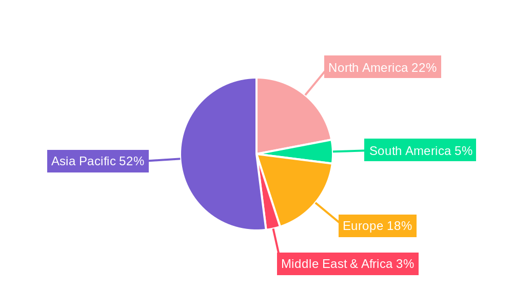
Emerging trends like the proliferation of 5G technology, the burgeoning IoT ecosystem, and advancements in automotive electronics are further accentuating the market's upward trajectory. Geographically, the Asia Pacific region, particularly China, is expected to dominate the market, owing to its strong manufacturing base and substantial investments in semiconductor production. However, North America and Europe also represent significant markets, driven by their own robust R&D initiatives and demand for high-performance computing. While the market benefits from strong drivers, potential restraints include the high cost of raw materials and stringent purity requirements, which necessitate sophisticated manufacturing processes. Key players like JX Metals, ULVAC, and Tosoh are actively engaged in innovation and capacity expansion to meet the escalating global demand for these critical semiconductor materials.
6n Copper Sputtering Targets For Semiconductor Market Concentration & Dynamics
The 6n Copper Sputtering Targets market for semiconductors is characterized by high concentration, with a few dominant players driving innovation and supply. This landscape is shaped by intense R&D investment and stringent quality requirements for ultra-high purity (UHP) materials. The innovation ecosystem is robust, driven by the constant demand for smaller, faster, and more efficient semiconductor devices. Regulatory frameworks are primarily driven by environmental, health, and safety (EHS) standards in material manufacturing and global trade policies influencing raw material sourcing and finished product distribution. Substitute products, while limited in the context of ultra-high purity copper for critical semiconductor applications, are generally not a significant threat due to the specific performance requirements. End-user trends heavily favor miniaturization, increased transistor density, and advanced packaging technologies, all of which necessitate superior sputtering target materials. Mergers and acquisitions (M&A) are sporadic but significant, often aimed at consolidating market share, acquiring intellectual property, or expanding geographical reach. For instance, recent M&A activities have seen key players seeking to integrate supply chains or secure critical raw material sources. Market share is closely guarded, with leading companies maintaining significant portions of the global UHP copper sputtering target market.
6n Copper Sputtering Targets For Semiconductor Industry Insights & Trends
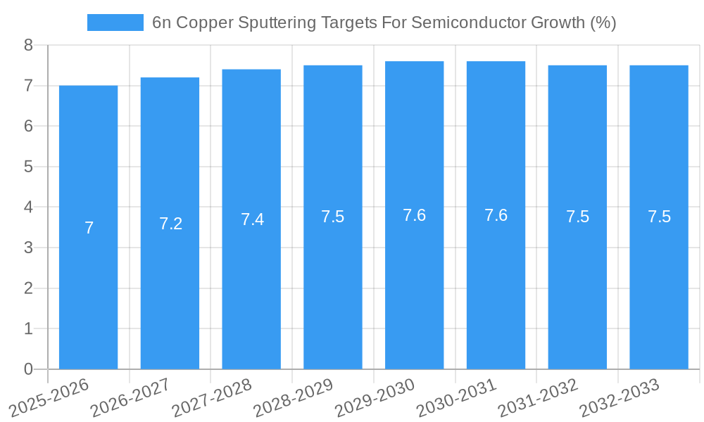
The 6n Copper Sputtering Targets for Semiconductor market is poised for substantial growth, driven by the insatiable demand for advanced electronic devices across diverse sectors. The market size for 6n copper sputtering targets for semiconductor applications was estimated to be $850 million in the base year of 2025 and is projected to reach $1,750 million by the end of the forecast period in 2033. This represents a compelling Compound Annual Growth Rate (CAGR) of approximately 9.25% throughout the study period of 2019–2033. The primary growth driver is the escalating demand for high-performance semiconductors used in 5G infrastructure, artificial intelligence (AI) processors, Internet of Things (IoT) devices, and advanced automotive electronics. As chip manufacturers push the boundaries of miniaturization and complexity, the need for ultra-high purity (UHP) 6n copper sputtering targets becomes paramount for achieving superior film quality, conductivity, and reliability in critical interconnect layers, under-bump metallization (UBM), and through-silicon vias (TSV). Technological disruptions, such as the advancement of eutectic bonding and advanced lithography techniques, further necessitate the development and widespread adoption of advanced sputtering target materials. Evolving consumer behaviors, including the increasing adoption of smart devices, electric vehicles, and immersive entertainment technologies, directly translate into a higher volume of semiconductor production, thus fueling the demand for these specialized materials. Furthermore, government initiatives and investments in domestic semiconductor manufacturing capabilities in key regions are also contributing to market expansion. The continuous pursuit of higher yields and lower defect rates in semiconductor fabrication processes reinforces the critical role of high-purity copper sputtering targets, making them indispensable components in the modern semiconductor supply chain. The industry is observing a trend towards larger wafer sizes, like 300mm type targets, to improve manufacturing efficiency and reduce costs per wafer, further influencing the demand dynamics for these materials.
Key Markets & Segments Leading 6n Copper Sputtering Targets For Semiconductor
The 6n Copper Sputtering Targets for Semiconductor market is experiencing robust growth across multiple key segments, with particular dominance observed in specific applications and wafer types.
Dominant Applications:
Cu Interconnect Seed Layer: This application stands as a cornerstone of the semiconductor industry, where 6n copper sputtering targets are indispensable for forming the initial seed layer for copper interconnects. The ever-increasing density of transistors and the need for faster signal transmission necessitate ultra-smooth, highly conductive copper films, making 6n purity a critical requirement.
- Drivers:
- Advancements in Chip Architecture: The transition to FinFET and GAAFET technologies, along with the push for smaller node sizes (e.g., 5nm, 3nm, and below), significantly increases the complexity and number of interconnect layers requiring high-quality copper deposition.
- Demand for High-Speed Computing: The proliferation of AI, high-performance computing (HPC), and advanced graphics processing units (GPUs) directly fuels the demand for semiconductors with superior interconnect performance.
- Economic Growth in Consumer Electronics: The sustained global demand for smartphones, laptops, and other consumer electronics ensures a consistent need for advanced interconnect technologies.
Under-Bump Metalization (UBM): UBM plays a crucial role in die-to-wafer and wafer-to-wafer bonding, particularly in advanced packaging solutions. 6n copper sputtering targets are vital for creating reliable and robust UBM layers that ensure excellent adhesion and electrical conductivity between the semiconductor die and the interconnect substrate.
- Drivers:
- Rise of Advanced Packaging: Technologies like 2.5D and 3D packaging, driven by the need for increased performance and reduced form factor, rely heavily on high-quality UBM for reliable interconnections.
- Growth in Mobile Devices and Wearables: The miniaturization and power efficiency demands of these devices necessitate advanced packaging techniques that benefit from superior UBM properties.
Through Silicon-via (TSV): TSV technology is critical for creating vertically interconnected semiconductor devices, enabling higher integration and performance. 6n copper sputtering targets are essential for the deposition of copper within the TSV structures, facilitating efficient electrical pathways through the silicon substrate.
- Drivers:
- High-Bandwidth Memory (HBM): HBM, a critical component in AI accelerators and high-performance computing, relies heavily on TSV technology for its dense and high-speed memory architecture.
- 3D IC Stacking: The increasing trend towards stacking multiple dies vertically to enhance performance and functionality makes TSV a key enabling technology.
Dominant Type:
- 300mm Type: The semiconductor industry has largely transitioned to 300mm wafer manufacturing. Consequently, sputtering targets designed for 300mm wafer processing dominate the market due to economies of scale and increased throughput in fabrication facilities. These larger targets are crucial for covering the entire surface of larger wafers efficiently and uniformly.
- Drivers:
- Economies of Scale: 300mm wafer fabrication plants offer significant cost advantages per chip compared to older 200mm facilities, leading to their widespread adoption.
- Increased Manufacturing Throughput: Larger wafers mean fewer processing steps per unit of silicon area, leading to higher overall manufacturing efficiency.
- Global Semiconductor Manufacturing Capacity: The concentration of advanced semiconductor foundries utilizing 300mm technology dictates the demand for corresponding sputtering target sizes.
Key Markets:
Cu Interconnect Seed Layer: This application stands as a cornerstone of the semiconductor industry, where 6n copper sputtering targets are indispensable for forming the initial seed layer for copper interconnects. The ever-increasing density of transistors and the need for faster signal transmission necessitate ultra-smooth, highly conductive copper films, making 6n purity a critical requirement.
- Drivers:
- Advancements in Chip Architecture: The transition to FinFET and GAAFET technologies, along with the push for smaller node sizes (e.g., 5nm, 3nm, and below), significantly increases the complexity and number of interconnect layers requiring high-quality copper deposition.
- Demand for High-Speed Computing: The proliferation of AI, high-performance computing (HPC), and advanced graphics processing units (GPUs) directly fuels the demand for semiconductors with superior interconnect performance.
- Economic Growth in Consumer Electronics: The sustained global demand for smartphones, laptops, and other consumer electronics ensures a consistent need for advanced interconnect technologies.
Under-Bump Metalization (UBM): UBM plays a crucial role in die-to-wafer and wafer-to-wafer bonding, particularly in advanced packaging solutions. 6n copper sputtering targets are vital for creating reliable and robust UBM layers that ensure excellent adhesion and electrical conductivity between the semiconductor die and the interconnect substrate.
- Drivers:
- Rise of Advanced Packaging: Technologies like 2.5D and 3D packaging, driven by the need for increased performance and reduced form factor, rely heavily on high-quality UBM for reliable interconnections.
- Growth in Mobile Devices and Wearables: The miniaturization and power efficiency demands of these devices necessitate advanced packaging techniques that benefit from superior UBM properties.
Through Silicon-via (TSV): TSV technology is critical for creating vertically interconnected semiconductor devices, enabling higher integration and performance. 6n copper sputtering targets are essential for the deposition of copper within the TSV structures, facilitating efficient electrical pathways through the silicon substrate.
- Drivers:
- High-Bandwidth Memory (HBM): HBM, a critical component in AI accelerators and high-performance computing, relies heavily on TSV technology for its dense and high-speed memory architecture.
- 3D IC Stacking: The increasing trend towards stacking multiple dies vertically to enhance performance and functionality makes TSV a key enabling technology.
- 300mm Type: The semiconductor industry has largely transitioned to 300mm wafer manufacturing. Consequently, sputtering targets designed for 300mm wafer processing dominate the market due to economies of scale and increased throughput in fabrication facilities. These larger targets are crucial for covering the entire surface of larger wafers efficiently and uniformly.
- Drivers:
- Economies of Scale: 300mm wafer fabrication plants offer significant cost advantages per chip compared to older 200mm facilities, leading to their widespread adoption.
- Increased Manufacturing Throughput: Larger wafers mean fewer processing steps per unit of silicon area, leading to higher overall manufacturing efficiency.
- Global Semiconductor Manufacturing Capacity: The concentration of advanced semiconductor foundries utilizing 300mm technology dictates the demand for corresponding sputtering target sizes.
- Drivers:
Key Markets:
While the market is global, Asia-Pacific, particularly Taiwan, South Korea, and China, emerges as the dominant region. This is due to the high concentration of leading semiconductor foundries and integrated device manufacturers (IDMs) operating state-of-the-art 300mm fabrication facilities. The robust demand from these regions for advanced semiconductor components directly translates into the leading position in the 6n copper sputtering targets market.
6n Copper Sputtering Targets For Semiconductor Product Developments
Recent product developments in 6n copper sputtering targets for semiconductors have focused on achieving even higher purity levels, reduced impurity concentrations, and improved microstructural homogeneity. Manufacturers are innovating to create targets with enhanced density and optimized grain structure, crucial for achieving defect-free films and superior electrical performance in advanced interconnects, UBM, and TSV applications. These advancements address the stringent requirements of sub-7nm semiconductor nodes and the growing demand for reliability in critical applications like AI and 5G. The competitive edge lies in the ability to consistently deliver targets that minimize sputtering issues like arcing and particulate generation, thereby improving wafer yields and reducing manufacturing costs for semiconductor foundries.
Challenges in the 6n Copper Sputtering Targets For Semiconductor Market
The 6n Copper Sputtering Targets market faces several significant challenges that can impact growth and profitability. Stringent purity requirements translate to complex and expensive manufacturing processes, limiting the number of qualified suppliers. Volatile raw material prices for high-purity copper can introduce cost instability. Furthermore, long lead times and complex supply chains for specialized materials can create bottlenecks. Intense competition from established players and the high barrier to entry for new entrants due to significant R&D and capital investment requirements also pose challenges. Finally, evolving semiconductor technology roadmaps necessitate continuous innovation and adaptation, requiring substantial investment in R&D to keep pace with the demands of shrinking process nodes and new device architectures.
Forces Driving 6n Copper Sputtering Targets For Semiconductor Growth
The growth of the 6n Copper Sputtering Targets market is propelled by several powerful forces. The relentless demand for enhanced semiconductor performance and miniaturization is a primary driver. Advancements in technologies like 5G, AI, and IoT require more sophisticated and higher-density integrated circuits, directly increasing the need for high-purity copper interconnects. Government initiatives and investments in domestic semiconductor manufacturing in various regions are creating significant market opportunities. The increasing complexity of chip designs, particularly the adoption of advanced packaging solutions like 3D ICs and HBM, further necessitates the use of ultra-high purity copper sputtering targets for reliable interconnections.
Challenges in the 6n Copper Sputtering Targets For Semiconductor Market
Looking beyond immediate hurdles, the long-term growth of the 6n Copper Sputtering Targets market will be shaped by ongoing technological evolution and strategic market positioning. The sustained push towards smaller semiconductor nodes will continue to demand materials with even greater purity and precision. Innovations in deposition techniques, such as atomic layer deposition (ALD) integrated with sputtering, could influence target requirements. Furthermore, strategic partnerships and collaborations between sputtering target manufacturers and leading semiconductor foundries will be crucial for co-developing next-generation materials tailored to future process needs. Market expansion into emerging semiconductor sectors and regions with growing manufacturing capabilities will also act as significant long-term growth catalysts.
Emerging Opportunities in 6n Copper Sputtering Targets For Semiconductor
Emerging opportunities within the 6n Copper Sputtering Targets market are plentiful and diverse. The burgeoning field of quantum computing and the development of specialized semiconductor chips for its infrastructure present a unique demand for ultra-high purity materials. The automotive sector's increasing reliance on advanced electronics, from autonomous driving systems to electric vehicle power management, offers a significant growth avenue. Furthermore, the continuous expansion of data centers and AI infrastructure creates a sustained demand for high-performance semiconductors, thereby driving the need for advanced sputtering targets. Opportunities also lie in developing novel sputtering target formulations and manufacturing processes that offer cost efficiencies without compromising purity, appealing to a broader segment of the market.
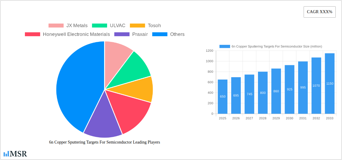
Leading Players in the 6n Copper Sputtering Targets For Semiconductor Sector
- JX Metals
- ULVAC
- Tosoh
- Honeywell Electronic Materials
- Praxair
- Konfoong Materials International
- GRIKIN Advanced Materials
- Changsha Xinkang
- Fujian Acetron New Materials
Key Milestones in 6n Copper Sputtering Targets For Semiconductor Industry
- 2019: Increased industry focus on sub-10nm process nodes, driving demand for higher purity 6n copper targets.
- 2020: Significant global investment announcements in advanced semiconductor manufacturing capacity, boosting future demand projections.
- 2021: Launch of new sputtering target formulations with improved microstructural control for enhanced film uniformity.
- 2022: Growing adoption of 300mm type targets across more advanced fabs globally.
- 2023: Key players announce expansions in R&D for next-generation sputtering materials to meet future technology nodes.
- 2024: Increased M&A activity aimed at consolidating market share and securing supply chains.
Strategic Outlook for 6n Copper Sputtering Targets For Semiconductor Market
The strategic outlook for the 6n Copper Sputtering Targets for Semiconductor market is overwhelmingly positive, driven by the foundational role of copper interconnects in next-generation semiconductor technologies. Key growth accelerators will include the continued expansion of AI, 5G, and automotive electronics, which will necessitate increasingly complex and high-density chip architectures. Manufacturers who can demonstrate consistent supply of ultra-high purity materials, coupled with advanced technological capabilities to meet sub-7nm node requirements, will command a premium. Strategic opportunities lie in forging deeper collaborations with leading foundries to co-develop tailored sputtering solutions and in expanding production capacity to meet the projected surge in demand. Diversification into emerging applications and maintaining a strong R&D pipeline for material innovation will be crucial for sustained market leadership.
6n Copper Sputtering Targets For Semiconductor Segmentation
-
1. Application
- 1.1. Cu Interconnect Seed Layer
- 1.2. Under-Bump Metalization (UBM)
- 1.3. Through Silicon-via (TSV)
- 1.4. Other
-
2. Type
- 2.1. 300mm Type
- 2.2. Other
6n Copper Sputtering Targets For Semiconductor Segmentation By Geography
-
1. North America
- 1.1. United States
- 1.2. Canada
- 1.3. Mexico
-
2. South America
- 2.1. Brazil
- 2.2. Argentina
- 2.3. Rest of South America
-
3. Europe
- 3.1. United Kingdom
- 3.2. Germany
- 3.3. France
- 3.4. Italy
- 3.5. Spain
- 3.6. Russia
- 3.7. Benelux
- 3.8. Nordics
- 3.9. Rest of Europe
-
4. Middle East & Africa
- 4.1. Turkey
- 4.2. Israel
- 4.3. GCC
- 4.4. North Africa
- 4.5. South Africa
- 4.6. Rest of Middle East & Africa
-
5. Asia Pacific
- 5.1. China
- 5.2. India
- 5.3. Japan
- 5.4. South Korea
- 5.5. ASEAN
- 5.6. Oceania
- 5.7. Rest of Asia Pacific
6n Copper Sputtering Targets For Semiconductor REPORT HIGHLIGHTS
| Aspects | Details |
|---|---|
| Study Period | 2019-2033 |
| Base Year | 2024 |
| Estimated Year | 2025 |
| Forecast Period | 2025-2033 |
| Historical Period | 2019-2024 |
| Growth Rate | CAGR of XXX% from 2019-2033 |
| Segmentation |
|
Table of Contents
- 1. Introduction
- 1.1. Research Scope
- 1.2. Market Segmentation
- 1.3. Research Methodology
- 1.4. Definitions and Assumptions
- 2. Executive Summary
- 2.1. Introduction
- 3. Market Dynamics
- 3.1. Introduction
- 3.2. Market Drivers
- 3.3. Market Restrains
- 3.4. Market Trends
- 4. Market Factor Analysis
- 4.1. Porters Five Forces
- 4.2. Supply/Value Chain
- 4.3. PESTEL analysis
- 4.4. Market Entropy
- 4.5. Patent/Trademark Analysis
- 5. Global 6n Copper Sputtering Targets For Semiconductor Analysis, Insights and Forecast, 2019-2031
- 5.1. Market Analysis, Insights and Forecast - by Application
- 5.1.1. Cu Interconnect Seed Layer
- 5.1.2. Under-Bump Metalization (UBM)
- 5.1.3. Through Silicon-via (TSV)
- 5.1.4. Other
- 5.2. Market Analysis, Insights and Forecast - by Type
- 5.2.1. 300mm Type
- 5.2.2. Other
- 5.3. Market Analysis, Insights and Forecast - by Region
- 5.3.1. North America
- 5.3.2. South America
- 5.3.3. Europe
- 5.3.4. Middle East & Africa
- 5.3.5. Asia Pacific
- 5.1. Market Analysis, Insights and Forecast - by Application
- 6. North America 6n Copper Sputtering Targets For Semiconductor Analysis, Insights and Forecast, 2019-2031
- 6.1. Market Analysis, Insights and Forecast - by Application
- 6.1.1. Cu Interconnect Seed Layer
- 6.1.2. Under-Bump Metalization (UBM)
- 6.1.3. Through Silicon-via (TSV)
- 6.1.4. Other
- 6.2. Market Analysis, Insights and Forecast - by Type
- 6.2.1. 300mm Type
- 6.2.2. Other
- 6.1. Market Analysis, Insights and Forecast - by Application
- 7. South America 6n Copper Sputtering Targets For Semiconductor Analysis, Insights and Forecast, 2019-2031
- 7.1. Market Analysis, Insights and Forecast - by Application
- 7.1.1. Cu Interconnect Seed Layer
- 7.1.2. Under-Bump Metalization (UBM)
- 7.1.3. Through Silicon-via (TSV)
- 7.1.4. Other
- 7.2. Market Analysis, Insights and Forecast - by Type
- 7.2.1. 300mm Type
- 7.2.2. Other
- 7.1. Market Analysis, Insights and Forecast - by Application
- 8. Europe 6n Copper Sputtering Targets For Semiconductor Analysis, Insights and Forecast, 2019-2031
- 8.1. Market Analysis, Insights and Forecast - by Application
- 8.1.1. Cu Interconnect Seed Layer
- 8.1.2. Under-Bump Metalization (UBM)
- 8.1.3. Through Silicon-via (TSV)
- 8.1.4. Other
- 8.2. Market Analysis, Insights and Forecast - by Type
- 8.2.1. 300mm Type
- 8.2.2. Other
- 8.1. Market Analysis, Insights and Forecast - by Application
- 9. Middle East & Africa 6n Copper Sputtering Targets For Semiconductor Analysis, Insights and Forecast, 2019-2031
- 9.1. Market Analysis, Insights and Forecast - by Application
- 9.1.1. Cu Interconnect Seed Layer
- 9.1.2. Under-Bump Metalization (UBM)
- 9.1.3. Through Silicon-via (TSV)
- 9.1.4. Other
- 9.2. Market Analysis, Insights and Forecast - by Type
- 9.2.1. 300mm Type
- 9.2.2. Other
- 9.1. Market Analysis, Insights and Forecast - by Application
- 10. Asia Pacific 6n Copper Sputtering Targets For Semiconductor Analysis, Insights and Forecast, 2019-2031
- 10.1. Market Analysis, Insights and Forecast - by Application
- 10.1.1. Cu Interconnect Seed Layer
- 10.1.2. Under-Bump Metalization (UBM)
- 10.1.3. Through Silicon-via (TSV)
- 10.1.4. Other
- 10.2. Market Analysis, Insights and Forecast - by Type
- 10.2.1. 300mm Type
- 10.2.2. Other
- 10.1. Market Analysis, Insights and Forecast - by Application
- 11. Competitive Analysis
- 11.1. Global Market Share Analysis 2024
- 11.2. Company Profiles
- 11.2.1 JX Metals
- 11.2.1.1. Overview
- 11.2.1.2. Products
- 11.2.1.3. SWOT Analysis
- 11.2.1.4. Recent Developments
- 11.2.1.5. Financials (Based on Availability)
- 11.2.2 ULVAC
- 11.2.2.1. Overview
- 11.2.2.2. Products
- 11.2.2.3. SWOT Analysis
- 11.2.2.4. Recent Developments
- 11.2.2.5. Financials (Based on Availability)
- 11.2.3 Tosoh
- 11.2.3.1. Overview
- 11.2.3.2. Products
- 11.2.3.3. SWOT Analysis
- 11.2.3.4. Recent Developments
- 11.2.3.5. Financials (Based on Availability)
- 11.2.4 Honeywell Electronic Materials
- 11.2.4.1. Overview
- 11.2.4.2. Products
- 11.2.4.3. SWOT Analysis
- 11.2.4.4. Recent Developments
- 11.2.4.5. Financials (Based on Availability)
- 11.2.5 Praxair
- 11.2.5.1. Overview
- 11.2.5.2. Products
- 11.2.5.3. SWOT Analysis
- 11.2.5.4. Recent Developments
- 11.2.5.5. Financials (Based on Availability)
- 11.2.6 Konfoong Materials International
- 11.2.6.1. Overview
- 11.2.6.2. Products
- 11.2.6.3. SWOT Analysis
- 11.2.6.4. Recent Developments
- 11.2.6.5. Financials (Based on Availability)
- 11.2.7 GRIKIN Advanced Materials
- 11.2.7.1. Overview
- 11.2.7.2. Products
- 11.2.7.3. SWOT Analysis
- 11.2.7.4. Recent Developments
- 11.2.7.5. Financials (Based on Availability)
- 11.2.8 Changsha Xinkang
- 11.2.8.1. Overview
- 11.2.8.2. Products
- 11.2.8.3. SWOT Analysis
- 11.2.8.4. Recent Developments
- 11.2.8.5. Financials (Based on Availability)
- 11.2.9 Fujian Acetron New Materials
- 11.2.9.1. Overview
- 11.2.9.2. Products
- 11.2.9.3. SWOT Analysis
- 11.2.9.4. Recent Developments
- 11.2.9.5. Financials (Based on Availability)
- 11.2.1 JX Metals
List of Figures
- Figure 1: Global 6n Copper Sputtering Targets For Semiconductor Revenue Breakdown (million, %) by Region 2024 & 2032
- Figure 2: North America 6n Copper Sputtering Targets For Semiconductor Revenue (million), by Application 2024 & 2032
- Figure 3: North America 6n Copper Sputtering Targets For Semiconductor Revenue Share (%), by Application 2024 & 2032
- Figure 4: North America 6n Copper Sputtering Targets For Semiconductor Revenue (million), by Type 2024 & 2032
- Figure 5: North America 6n Copper Sputtering Targets For Semiconductor Revenue Share (%), by Type 2024 & 2032
- Figure 6: North America 6n Copper Sputtering Targets For Semiconductor Revenue (million), by Country 2024 & 2032
- Figure 7: North America 6n Copper Sputtering Targets For Semiconductor Revenue Share (%), by Country 2024 & 2032
- Figure 8: South America 6n Copper Sputtering Targets For Semiconductor Revenue (million), by Application 2024 & 2032
- Figure 9: South America 6n Copper Sputtering Targets For Semiconductor Revenue Share (%), by Application 2024 & 2032
- Figure 10: South America 6n Copper Sputtering Targets For Semiconductor Revenue (million), by Type 2024 & 2032
- Figure 11: South America 6n Copper Sputtering Targets For Semiconductor Revenue Share (%), by Type 2024 & 2032
- Figure 12: South America 6n Copper Sputtering Targets For Semiconductor Revenue (million), by Country 2024 & 2032
- Figure 13: South America 6n Copper Sputtering Targets For Semiconductor Revenue Share (%), by Country 2024 & 2032
- Figure 14: Europe 6n Copper Sputtering Targets For Semiconductor Revenue (million), by Application 2024 & 2032
- Figure 15: Europe 6n Copper Sputtering Targets For Semiconductor Revenue Share (%), by Application 2024 & 2032
- Figure 16: Europe 6n Copper Sputtering Targets For Semiconductor Revenue (million), by Type 2024 & 2032
- Figure 17: Europe 6n Copper Sputtering Targets For Semiconductor Revenue Share (%), by Type 2024 & 2032
- Figure 18: Europe 6n Copper Sputtering Targets For Semiconductor Revenue (million), by Country 2024 & 2032
- Figure 19: Europe 6n Copper Sputtering Targets For Semiconductor Revenue Share (%), by Country 2024 & 2032
- Figure 20: Middle East & Africa 6n Copper Sputtering Targets For Semiconductor Revenue (million), by Application 2024 & 2032
- Figure 21: Middle East & Africa 6n Copper Sputtering Targets For Semiconductor Revenue Share (%), by Application 2024 & 2032
- Figure 22: Middle East & Africa 6n Copper Sputtering Targets For Semiconductor Revenue (million), by Type 2024 & 2032
- Figure 23: Middle East & Africa 6n Copper Sputtering Targets For Semiconductor Revenue Share (%), by Type 2024 & 2032
- Figure 24: Middle East & Africa 6n Copper Sputtering Targets For Semiconductor Revenue (million), by Country 2024 & 2032
- Figure 25: Middle East & Africa 6n Copper Sputtering Targets For Semiconductor Revenue Share (%), by Country 2024 & 2032
- Figure 26: Asia Pacific 6n Copper Sputtering Targets For Semiconductor Revenue (million), by Application 2024 & 2032
- Figure 27: Asia Pacific 6n Copper Sputtering Targets For Semiconductor Revenue Share (%), by Application 2024 & 2032
- Figure 28: Asia Pacific 6n Copper Sputtering Targets For Semiconductor Revenue (million), by Type 2024 & 2032
- Figure 29: Asia Pacific 6n Copper Sputtering Targets For Semiconductor Revenue Share (%), by Type 2024 & 2032
- Figure 30: Asia Pacific 6n Copper Sputtering Targets For Semiconductor Revenue (million), by Country 2024 & 2032
- Figure 31: Asia Pacific 6n Copper Sputtering Targets For Semiconductor Revenue Share (%), by Country 2024 & 2032
List of Tables
- Table 1: Global 6n Copper Sputtering Targets For Semiconductor Revenue million Forecast, by Region 2019 & 2032
- Table 2: Global 6n Copper Sputtering Targets For Semiconductor Revenue million Forecast, by Application 2019 & 2032
- Table 3: Global 6n Copper Sputtering Targets For Semiconductor Revenue million Forecast, by Type 2019 & 2032
- Table 4: Global 6n Copper Sputtering Targets For Semiconductor Revenue million Forecast, by Region 2019 & 2032
- Table 5: Global 6n Copper Sputtering Targets For Semiconductor Revenue million Forecast, by Application 2019 & 2032
- Table 6: Global 6n Copper Sputtering Targets For Semiconductor Revenue million Forecast, by Type 2019 & 2032
- Table 7: Global 6n Copper Sputtering Targets For Semiconductor Revenue million Forecast, by Country 2019 & 2032
- Table 8: United States 6n Copper Sputtering Targets For Semiconductor Revenue (million) Forecast, by Application 2019 & 2032
- Table 9: Canada 6n Copper Sputtering Targets For Semiconductor Revenue (million) Forecast, by Application 2019 & 2032
- Table 10: Mexico 6n Copper Sputtering Targets For Semiconductor Revenue (million) Forecast, by Application 2019 & 2032
- Table 11: Global 6n Copper Sputtering Targets For Semiconductor Revenue million Forecast, by Application 2019 & 2032
- Table 12: Global 6n Copper Sputtering Targets For Semiconductor Revenue million Forecast, by Type 2019 & 2032
- Table 13: Global 6n Copper Sputtering Targets For Semiconductor Revenue million Forecast, by Country 2019 & 2032
- Table 14: Brazil 6n Copper Sputtering Targets For Semiconductor Revenue (million) Forecast, by Application 2019 & 2032
- Table 15: Argentina 6n Copper Sputtering Targets For Semiconductor Revenue (million) Forecast, by Application 2019 & 2032
- Table 16: Rest of South America 6n Copper Sputtering Targets For Semiconductor Revenue (million) Forecast, by Application 2019 & 2032
- Table 17: Global 6n Copper Sputtering Targets For Semiconductor Revenue million Forecast, by Application 2019 & 2032
- Table 18: Global 6n Copper Sputtering Targets For Semiconductor Revenue million Forecast, by Type 2019 & 2032
- Table 19: Global 6n Copper Sputtering Targets For Semiconductor Revenue million Forecast, by Country 2019 & 2032
- Table 20: United Kingdom 6n Copper Sputtering Targets For Semiconductor Revenue (million) Forecast, by Application 2019 & 2032
- Table 21: Germany 6n Copper Sputtering Targets For Semiconductor Revenue (million) Forecast, by Application 2019 & 2032
- Table 22: France 6n Copper Sputtering Targets For Semiconductor Revenue (million) Forecast, by Application 2019 & 2032
- Table 23: Italy 6n Copper Sputtering Targets For Semiconductor Revenue (million) Forecast, by Application 2019 & 2032
- Table 24: Spain 6n Copper Sputtering Targets For Semiconductor Revenue (million) Forecast, by Application 2019 & 2032
- Table 25: Russia 6n Copper Sputtering Targets For Semiconductor Revenue (million) Forecast, by Application 2019 & 2032
- Table 26: Benelux 6n Copper Sputtering Targets For Semiconductor Revenue (million) Forecast, by Application 2019 & 2032
- Table 27: Nordics 6n Copper Sputtering Targets For Semiconductor Revenue (million) Forecast, by Application 2019 & 2032
- Table 28: Rest of Europe 6n Copper Sputtering Targets For Semiconductor Revenue (million) Forecast, by Application 2019 & 2032
- Table 29: Global 6n Copper Sputtering Targets For Semiconductor Revenue million Forecast, by Application 2019 & 2032
- Table 30: Global 6n Copper Sputtering Targets For Semiconductor Revenue million Forecast, by Type 2019 & 2032
- Table 31: Global 6n Copper Sputtering Targets For Semiconductor Revenue million Forecast, by Country 2019 & 2032
- Table 32: Turkey 6n Copper Sputtering Targets For Semiconductor Revenue (million) Forecast, by Application 2019 & 2032
- Table 33: Israel 6n Copper Sputtering Targets For Semiconductor Revenue (million) Forecast, by Application 2019 & 2032
- Table 34: GCC 6n Copper Sputtering Targets For Semiconductor Revenue (million) Forecast, by Application 2019 & 2032
- Table 35: North Africa 6n Copper Sputtering Targets For Semiconductor Revenue (million) Forecast, by Application 2019 & 2032
- Table 36: South Africa 6n Copper Sputtering Targets For Semiconductor Revenue (million) Forecast, by Application 2019 & 2032
- Table 37: Rest of Middle East & Africa 6n Copper Sputtering Targets For Semiconductor Revenue (million) Forecast, by Application 2019 & 2032
- Table 38: Global 6n Copper Sputtering Targets For Semiconductor Revenue million Forecast, by Application 2019 & 2032
- Table 39: Global 6n Copper Sputtering Targets For Semiconductor Revenue million Forecast, by Type 2019 & 2032
- Table 40: Global 6n Copper Sputtering Targets For Semiconductor Revenue million Forecast, by Country 2019 & 2032
- Table 41: China 6n Copper Sputtering Targets For Semiconductor Revenue (million) Forecast, by Application 2019 & 2032
- Table 42: India 6n Copper Sputtering Targets For Semiconductor Revenue (million) Forecast, by Application 2019 & 2032
- Table 43: Japan 6n Copper Sputtering Targets For Semiconductor Revenue (million) Forecast, by Application 2019 & 2032
- Table 44: South Korea 6n Copper Sputtering Targets For Semiconductor Revenue (million) Forecast, by Application 2019 & 2032
- Table 45: ASEAN 6n Copper Sputtering Targets For Semiconductor Revenue (million) Forecast, by Application 2019 & 2032
- Table 46: Oceania 6n Copper Sputtering Targets For Semiconductor Revenue (million) Forecast, by Application 2019 & 2032
- Table 47: Rest of Asia Pacific 6n Copper Sputtering Targets For Semiconductor Revenue (million) Forecast, by Application 2019 & 2032
Frequently Asked Questions
1. What is the projected Compound Annual Growth Rate (CAGR) of the 6n Copper Sputtering Targets For Semiconductor?
The projected CAGR is approximately XXX%.
2. Which companies are prominent players in the 6n Copper Sputtering Targets For Semiconductor?
Key companies in the market include JX Metals, ULVAC, Tosoh, Honeywell Electronic Materials, Praxair, Konfoong Materials International, GRIKIN Advanced Materials, Changsha Xinkang, Fujian Acetron New Materials.
3. What are the main segments of the 6n Copper Sputtering Targets For Semiconductor?
The market segments include Application, Type.
4. Can you provide details about the market size?
The market size is estimated to be USD XXX million as of 2022.
5. What are some drivers contributing to market growth?
N/A
6. What are the notable trends driving market growth?
N/A
7. Are there any restraints impacting market growth?
N/A
8. Can you provide examples of recent developments in the market?
N/A
9. What pricing options are available for accessing the report?
Pricing options include single-user, multi-user, and enterprise licenses priced at USD 4250.00, USD 6375.00, and USD 8500.00 respectively.
10. Is the market size provided in terms of value or volume?
The market size is provided in terms of value, measured in million.
11. Are there any specific market keywords associated with the report?
Yes, the market keyword associated with the report is "6n Copper Sputtering Targets For Semiconductor," which aids in identifying and referencing the specific market segment covered.
12. How do I determine which pricing option suits my needs best?
The pricing options vary based on user requirements and access needs. Individual users may opt for single-user licenses, while businesses requiring broader access may choose multi-user or enterprise licenses for cost-effective access to the report.
13. Are there any additional resources or data provided in the 6n Copper Sputtering Targets For Semiconductor report?
While the report offers comprehensive insights, it's advisable to review the specific contents or supplementary materials provided to ascertain if additional resources or data are available.
14. How can I stay updated on further developments or reports in the 6n Copper Sputtering Targets For Semiconductor?
To stay informed about further developments, trends, and reports in the 6n Copper Sputtering Targets For Semiconductor, consider subscribing to industry newsletters, following relevant companies and organizations, or regularly checking reputable industry news sources and publications.
Methodology
Step 1 - Identification of Relevant Samples Size from Population Database


Step 2 - Approaches for Defining Global Market Size (Value, Volume* & Price*)

Note*: In applicable scenarios
Step 3 - Data Sources
Primary Research
- Web Analytics
- Survey Reports
- Research Institute
- Latest Research Reports
- Opinion Leaders
Secondary Research
- Annual Reports
- White Paper
- Latest Press Release
- Industry Association
- Paid Database
- Investor Presentations

Step 4 - Data Triangulation
Involves using different sources of information in order to increase the validity of a study
These sources are likely to be stakeholders in a program - participants, other researchers, program staff, other community members, and so on.
Then we put all data in single framework & apply various statistical tools to find out the dynamic on the market.
During the analysis stage, feedback from the stakeholder groups would be compared to determine areas of agreement as well as areas of divergence
