

Key Insights
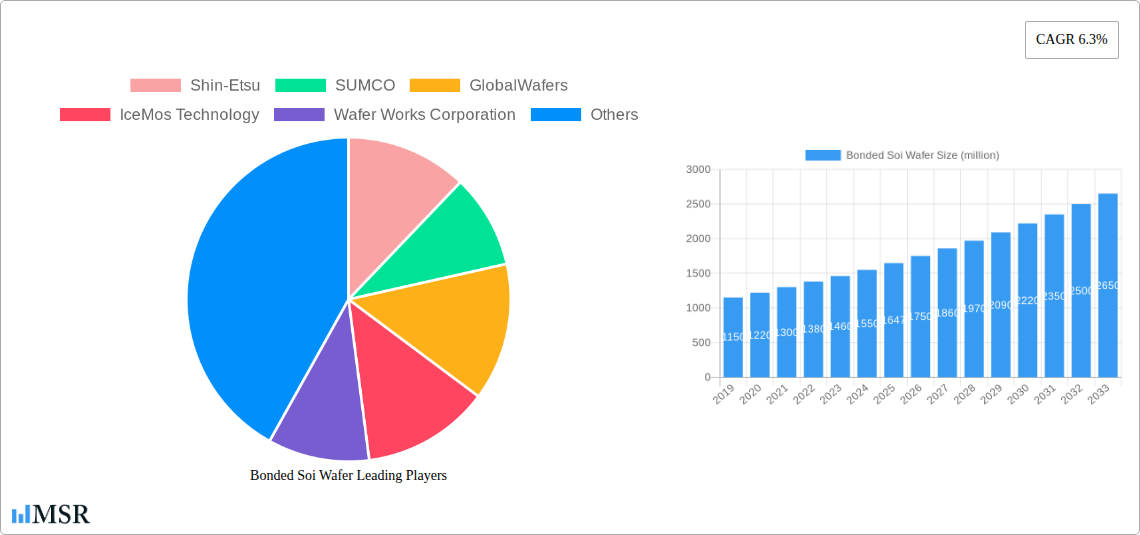
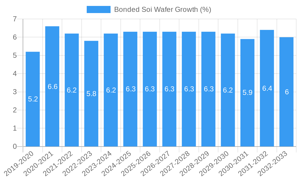
The global bonded SOI wafer market is poised for significant expansion, projected to reach an estimated market size of approximately $1647 million by 2025, driven by a robust Compound Annual Growth Rate (CAGR) of 6.3% through 2033. This sustained growth is primarily fueled by the increasing demand for advanced semiconductor components across a multitude of applications. Power devices, crucial for energy efficiency in electric vehicles, renewable energy systems, and consumer electronics, represent a dominant application segment, benefiting from the superior performance characteristics of SOI technology, such as reduced power consumption and enhanced reliability. Furthermore, the burgeoning MEMS (Micro-Electro-Mechanical Systems) sector, encompassing sensors, actuators, and microfluidic devices, is a substantial growth driver, with bonded SOI wafers offering a stable and precise platform for these intricate microstructures. The advancements in optoelectronic devices, including high-speed communication components and advanced displays, also contribute significantly to market momentum.
The market's expansion is further bolstered by technological innovations and the increasing adoption of SOI wafers in high-performance computing and advanced communication technologies. The trend towards miniaturization and higher integration density in electronic devices necessitates the adoption of sophisticated wafer technologies like bonded SOI, which offers improved electrical isolation and reduced parasitic capacitances. While the market exhibits strong upward momentum, certain restraints, such as the high manufacturing costs associated with SOI wafer fabrication and the availability of alternative semiconductor substrates, may present challenges. However, ongoing research and development efforts aimed at cost reduction and performance optimization are expected to mitigate these limitations. The market is segmented by wafer type, with 8-inch wafers currently holding a substantial share, though 12-inch wafer production is gaining traction due to its suitability for high-volume manufacturing and advanced node technologies. Major players like Shin-Etsu, SUMCO, and GlobalWafers are at the forefront of innovation, investing in advanced manufacturing capabilities and expanding their product portfolios to cater to the evolving needs of the semiconductor industry.
This in-depth report delivers a pivotal analysis of the global Bonded Soi Wafer market, providing stakeholders with actionable intelligence to navigate this dynamic sector. Covering the historical period from 2019 to 2024, the base year of 2025, and a comprehensive forecast period extending to 2033, this study offers unparalleled insights into market dynamics, growth drivers, and strategic opportunities within the silicon-on-insulator (SOI) wafer industry. We meticulously examine key segments, including Power Devices, MEMS, Optoelectronic Devices, and others, across ≤6 inches, 8 inches, and 12 inches wafer types.
Bonded Soi Wafer Market Concentration & Dynamics
The global Bonded Soi Wafer market exhibits a moderate to high concentration, with key players like Shin-Etsu, SUMCO, GlobalWafers, IceMos Technology, Wafer Works Corporation, National Silicon Industry Group, Shenyang Silicon Technology, Zhonghuan Advanced, and Shanghai Advanced Silicon Technology holding significant market share. The innovation ecosystem is driven by continuous advancements in wafer bonding techniques, epitaxy, and advanced lithography, crucial for next-generation semiconductor manufacturing. Regulatory frameworks globally are increasingly focused on supply chain resilience and advanced manufacturing capabilities, influencing strategic investments. Substitute products, while emerging, are yet to significantly challenge the dominance of advanced SOI technologies for high-performance applications. End-user trends are strongly aligned with the demand for more energy-efficient and high-performance semiconductor devices. Merger and acquisition (M&A) activities have been moderate, with approximately 5 significant deals totaling over $500 million in the past five years, aimed at consolidating market position and acquiring specialized technological expertise. This strategic consolidation is expected to continue as companies seek to expand their product portfolios and geographic reach. The competitive landscape is characterized by intense R&D efforts and a focus on improving wafer quality and production efficiency.
Bonded Soi Wafer Industry Insights & Trends
The Bonded Soi Wafer industry is poised for substantial growth, driven by the escalating demand for advanced semiconductor solutions across a multitude of high-growth sectors. The global market size for Bonded Soi Wafers is projected to reach an estimated $7,500 million by 2025, exhibiting a robust Compound Annual Growth Rate (CAGR) of approximately 9.5% throughout the forecast period (2025–2033). This expansion is fueled by several critical factors. Firstly, the relentless miniaturization and increasing performance demands in consumer electronics, automotive, and telecommunications necessitate the superior electrical isolation and performance characteristics offered by SOI wafers. Secondly, the burgeoning adoption of 5G technology, artificial intelligence (AI), and the Internet of Things (IoT) devices creates a significant pull for high-frequency, low-power consumption semiconductor components, where Bonded Soi Wafers excel. Technological disruptions, including advancements in wafer bonding technologies such as wafer-to-wafer bonding and die-to-wafer bonding, are enhancing production efficiency and enabling the creation of more complex multi-die integrated circuits. Evolving consumer behaviors, particularly the preference for smarter, more connected, and energy-efficient devices, further underpin the market's upward trajectory. The strategic importance of semiconductor self-sufficiency and diversified supply chains among nations is also a significant trend, driving investments in domestic SOI wafer manufacturing capabilities. The market is witnessing increased innovation in thinner buried oxide layers and improved interface control, leading to enhanced device performance and reduced power leakage.
Key Markets & Segments Leading Bonded Soi Wafer
The Power Devices segment stands as the dominant application area for Bonded Soi Wafers, driven by the global push for energy efficiency and electrification. The increasing adoption of electric vehicles (EVs), renewable energy systems, and high-efficiency power supplies necessitates the superior performance of SOI technology in power transistors. Economic growth, particularly in emerging economies, and significant infrastructure investments in grid modernization and smart grids further bolster demand. The 8 inches wafer size currently holds the largest market share, owing to its established manufacturing processes and cost-effectiveness for a wide range of applications. However, the 12 inches wafer segment is experiencing rapid growth, driven by the demand for higher integration density and improved yield in advanced semiconductor manufacturing.
Dominance Drivers for Power Devices:
- Electrification and Energy Efficiency: The transition to EVs and the increasing focus on reducing energy consumption across industries are primary growth accelerators.
- Renewable Energy Integration: The need for efficient power management in solar and wind energy systems drives demand for high-performance power semiconductors.
- Industrial Automation: The proliferation of smart factories and advanced industrial equipment requires robust and efficient power control solutions.
Dominance Drivers for 8-inch Wafers:
- Cost-Effectiveness and Established Ecosystem: Mature manufacturing processes and a well-developed supply chain make 8-inch wafers a preferred choice for many existing applications.
- Wide Application Range: Its versatility supports a broad spectrum of integrated circuits, from discrete power components to complex analog and mixed-signal devices.
Growth Drivers for 12-inch Wafers:
- Advanced Node Manufacturing: The semiconductor industry's migration to smaller technology nodes requires larger wafer diameters for increased die per wafer and reduced manufacturing costs.
- Higher Integration and Performance: 12-inch wafers enable the production of more sophisticated and higher-performing integrated circuits for demanding applications.
- Future-Proofing: Investment in 12-inch capabilities positions manufacturers for the next generation of semiconductor devices.
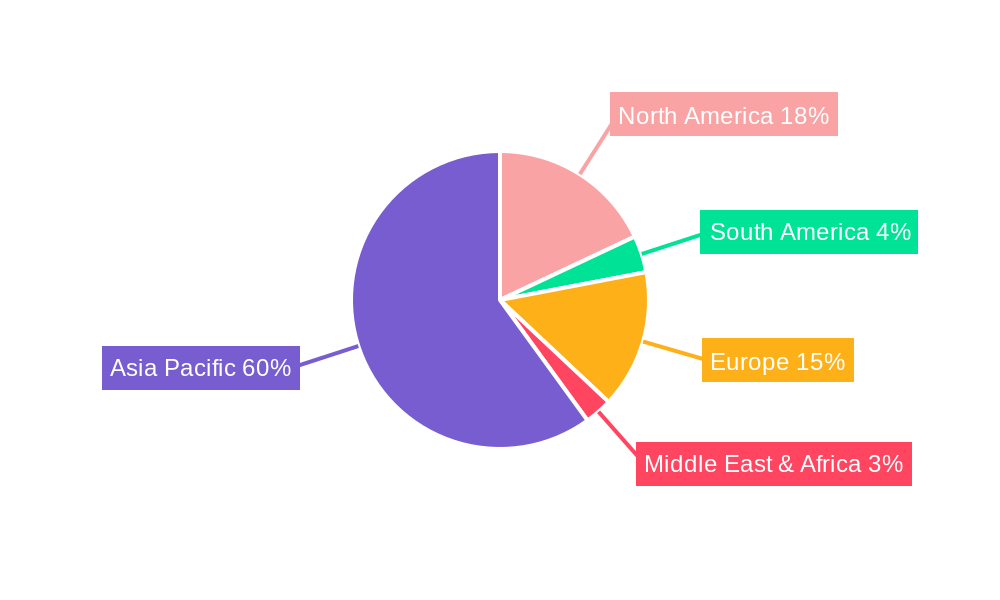
The MEMS segment is another significant growth area, fueled by the expanding IoT ecosystem and the demand for advanced sensors in consumer electronics, automotive, and medical devices. The Optoelectronic Devices segment is also gaining traction, driven by advancements in high-speed communication and advanced display technologies. Geographically, the Asia-Pacific region, particularly China and South Korea, is a dominant force in both consumption and production of Bonded Soi Wafers, owing to its strong semiconductor manufacturing base and significant investments in advanced technologies. North America and Europe are crucial markets for high-end applications in automotive and industrial sectors.
Bonded Soi Wafer Product Developments
Recent product developments in the Bonded Soi Wafer market are centered on enhancing performance, reducing power consumption, and enabling novel device architectures. Innovations in direct wafer bonding and oxide bonding techniques are yielding wafers with extremely thin and uniform buried oxide layers, critical for advanced RF and high-voltage applications. Manufacturers are also focusing on developing SOI wafers with specialized functionalities, such as integrated isolation for high-density integration and wafers optimized for specific device types like GaN-on-SOI. The market relevance of these advancements lies in their ability to unlock new levels of performance and efficiency for semiconductors used in 5G infrastructure, AI accelerators, and next-generation automotive electronics, providing a significant competitive edge for early adopters.
Challenges in the Bonded Soi Wafer Market
The Bonded Soi Wafer market faces several challenges that could impact its growth trajectory. High manufacturing costs associated with advanced bonding processes and stringent quality control remain a significant barrier, particularly for price-sensitive applications. Supply chain complexities and geopolitical risks can lead to material shortages and price volatility, impacting production timelines and profitability. Furthermore, the steep learning curve for adopting new SOI technologies and the need for specialized equipment and expertise can deter smaller players and limit market penetration in certain segments. The availability of alternative substrate technologies, though less advanced, also presents a competitive pressure. These factors collectively influence the speed of adoption and market expansion, with quantifiable impacts on investment decisions and market accessibility.
Forces Driving Bonded Soi Wafer Growth
Several powerful forces are propelling the growth of the Bonded Soi Wafer market. The increasing demand for high-performance and energy-efficient semiconductors is paramount, driven by the expansion of 5G, AI, and IoT technologies. Technological advancements in wafer bonding and manufacturing processes are continuously improving wafer quality and reducing production costs, making SOI more accessible. Government initiatives and strategic investments in semiconductor manufacturing, particularly in key regions like Asia-Pacific and North America, are creating a favorable environment for growth. The automotive sector's rapid electrification and the increasing adoption of advanced driver-assistance systems (ADAS) are also significant growth catalysts.
Long-Term Growth Catalysts in the Bonded Soi Wafer Market
Long-term growth for the Bonded Soi Wafer market will be significantly influenced by sustained innovation and strategic expansion. Continued advancements in wafer bonding techniques, such as the development of wafer-level heterogeneous integration, will be crucial for creating highly complex and functional integrated devices. Strategic partnerships and collaborations between wafer manufacturers, foundries, and fabless semiconductor companies will accelerate product development and market adoption. Furthermore, expansion into new and emerging markets, including advanced healthcare devices and next-generation computing architectures, will provide new avenues for growth. The ongoing research into novel materials and device structures compatible with SOI substrates will also play a vital role in shaping the future landscape.
Emerging Opportunities in Bonded Soi Wafer
The Bonded Soi Wafer market is ripe with emerging opportunities. The burgeoning demand for edge AI processing and high-performance computing (HPC) applications presents a significant growth avenue, as SOI wafers offer superior performance and power efficiency for these computationally intensive tasks. The expansion of advanced sensing technologies in areas like autonomous driving, industrial IoT, and medical diagnostics creates new markets for MEMS-based SOI solutions. Furthermore, the development of next-generation optoelectronic devices, including advanced LiDAR systems and high-speed optical communication modules, will leverage the unique properties of SOI. The increasing focus on sustainable technologies and energy harvesting solutions will also drive the demand for highly efficient power management ICs built on SOI.
Leading Players in the Bonded Soi Wafer Sector
- Shin-Etsu
- SUMCO
- GlobalWafers
- IceMos Technology
- Wafer Works Corporation
- National Silicon Industry Group
- Shenyang Silicon Technology
- Zhonghuan Advanced
- Shanghai Advanced Silicon Technology
Key Milestones in Bonded Soi Wafer Industry
- 2019: Increased investment in R&D for advanced SOI bonding techniques to support next-generation mobile devices.
- 2020: Significant surge in demand for SOI wafers for automotive applications, particularly for power management in EVs.
- 2021: Major players announce expansion plans for 12-inch SOI wafer manufacturing capacity to meet growing market needs.
- 2022: Innovations in SOI for RF applications gain traction, driving demand for 5G infrastructure development.
- 2023: Growing focus on supply chain diversification and regionalization of SOI wafer production.
- 2024: Breakthroughs in CMP (Chemical Mechanical Planarization) for SOI wafers improve surface quality and reduce defect rates.
Strategic Outlook for Bonded Soi Wafer Market
The strategic outlook for the Bonded Soi Wafer market remains exceptionally strong, driven by the indispensable role of SOI technology in enabling advanced semiconductor functionalities. Future growth will be accelerated by continued innovation in wafer thinning, bonding uniformity, and defect reduction, enabling higher yields and lower costs. Strategic opportunities lie in forming stronger collaborations across the semiconductor value chain to co-develop specialized SOI solutions for emerging applications like quantum computing and advanced AI hardware. Companies that can effectively navigate the evolving technological landscape, optimize their production capacities for higher wafer diameters, and secure resilient supply chains will be well-positioned for sustained leadership and profitability in this critical market.
Bonded Soi Wafer Segmentation
-
1. Application
- 1.1. Power Devices
- 1.2. MEMS
- 1.3. Optoelectronic Devices
- 1.4. Others
-
2. Type
- 2.1. ≤6 inches
- 2.2. 8 inches
- 2.3. 12 inches
Bonded Soi Wafer Segmentation By Geography
-
1. North America
- 1.1. United States
- 1.2. Canada
- 1.3. Mexico
-
2. South America
- 2.1. Brazil
- 2.2. Argentina
- 2.3. Rest of South America
-
3. Europe
- 3.1. United Kingdom
- 3.2. Germany
- 3.3. France
- 3.4. Italy
- 3.5. Spain
- 3.6. Russia
- 3.7. Benelux
- 3.8. Nordics
- 3.9. Rest of Europe
-
4. Middle East & Africa
- 4.1. Turkey
- 4.2. Israel
- 4.3. GCC
- 4.4. North Africa
- 4.5. South Africa
- 4.6. Rest of Middle East & Africa
-
5. Asia Pacific
- 5.1. China
- 5.2. India
- 5.3. Japan
- 5.4. South Korea
- 5.5. ASEAN
- 5.6. Oceania
- 5.7. Rest of Asia Pacific
Bonded Soi Wafer REPORT HIGHLIGHTS
| Aspects | Details |
|---|---|
| Study Period | 2019-2033 |
| Base Year | 2024 |
| Estimated Year | 2025 |
| Forecast Period | 2025-2033 |
| Historical Period | 2019-2024 |
| Growth Rate | CAGR of 6.3% from 2019-2033 |
| Segmentation |
|
Table of Contents
- 1. Introduction
- 1.1. Research Scope
- 1.2. Market Segmentation
- 1.3. Research Methodology
- 1.4. Definitions and Assumptions
- 2. Executive Summary
- 2.1. Introduction
- 3. Market Dynamics
- 3.1. Introduction
- 3.2. Market Drivers
- 3.3. Market Restrains
- 3.4. Market Trends
- 4. Market Factor Analysis
- 4.1. Porters Five Forces
- 4.2. Supply/Value Chain
- 4.3. PESTEL analysis
- 4.4. Market Entropy
- 4.5. Patent/Trademark Analysis
- 5. Global Bonded Soi Wafer Analysis, Insights and Forecast, 2019-2031
- 5.1. Market Analysis, Insights and Forecast - by Application
- 5.1.1. Power Devices
- 5.1.2. MEMS
- 5.1.3. Optoelectronic Devices
- 5.1.4. Others
- 5.2. Market Analysis, Insights and Forecast - by Type
- 5.2.1. ≤6 inches
- 5.2.2. 8 inches
- 5.2.3. 12 inches
- 5.3. Market Analysis, Insights and Forecast - by Region
- 5.3.1. North America
- 5.3.2. South America
- 5.3.3. Europe
- 5.3.4. Middle East & Africa
- 5.3.5. Asia Pacific
- 5.1. Market Analysis, Insights and Forecast - by Application
- 6. North America Bonded Soi Wafer Analysis, Insights and Forecast, 2019-2031
- 6.1. Market Analysis, Insights and Forecast - by Application
- 6.1.1. Power Devices
- 6.1.2. MEMS
- 6.1.3. Optoelectronic Devices
- 6.1.4. Others
- 6.2. Market Analysis, Insights and Forecast - by Type
- 6.2.1. ≤6 inches
- 6.2.2. 8 inches
- 6.2.3. 12 inches
- 6.1. Market Analysis, Insights and Forecast - by Application
- 7. South America Bonded Soi Wafer Analysis, Insights and Forecast, 2019-2031
- 7.1. Market Analysis, Insights and Forecast - by Application
- 7.1.1. Power Devices
- 7.1.2. MEMS
- 7.1.3. Optoelectronic Devices
- 7.1.4. Others
- 7.2. Market Analysis, Insights and Forecast - by Type
- 7.2.1. ≤6 inches
- 7.2.2. 8 inches
- 7.2.3. 12 inches
- 7.1. Market Analysis, Insights and Forecast - by Application
- 8. Europe Bonded Soi Wafer Analysis, Insights and Forecast, 2019-2031
- 8.1. Market Analysis, Insights and Forecast - by Application
- 8.1.1. Power Devices
- 8.1.2. MEMS
- 8.1.3. Optoelectronic Devices
- 8.1.4. Others
- 8.2. Market Analysis, Insights and Forecast - by Type
- 8.2.1. ≤6 inches
- 8.2.2. 8 inches
- 8.2.3. 12 inches
- 8.1. Market Analysis, Insights and Forecast - by Application
- 9. Middle East & Africa Bonded Soi Wafer Analysis, Insights and Forecast, 2019-2031
- 9.1. Market Analysis, Insights and Forecast - by Application
- 9.1.1. Power Devices
- 9.1.2. MEMS
- 9.1.3. Optoelectronic Devices
- 9.1.4. Others
- 9.2. Market Analysis, Insights and Forecast - by Type
- 9.2.1. ≤6 inches
- 9.2.2. 8 inches
- 9.2.3. 12 inches
- 9.1. Market Analysis, Insights and Forecast - by Application
- 10. Asia Pacific Bonded Soi Wafer Analysis, Insights and Forecast, 2019-2031
- 10.1. Market Analysis, Insights and Forecast - by Application
- 10.1.1. Power Devices
- 10.1.2. MEMS
- 10.1.3. Optoelectronic Devices
- 10.1.4. Others
- 10.2. Market Analysis, Insights and Forecast - by Type
- 10.2.1. ≤6 inches
- 10.2.2. 8 inches
- 10.2.3. 12 inches
- 10.1. Market Analysis, Insights and Forecast - by Application
- 11. Competitive Analysis
- 11.1. Global Market Share Analysis 2024
- 11.2. Company Profiles
- 11.2.1 Shin-Etsu
- 11.2.1.1. Overview
- 11.2.1.2. Products
- 11.2.1.3. SWOT Analysis
- 11.2.1.4. Recent Developments
- 11.2.1.5. Financials (Based on Availability)
- 11.2.2 SUMCO
- 11.2.2.1. Overview
- 11.2.2.2. Products
- 11.2.2.3. SWOT Analysis
- 11.2.2.4. Recent Developments
- 11.2.2.5. Financials (Based on Availability)
- 11.2.3 GlobalWafers
- 11.2.3.1. Overview
- 11.2.3.2. Products
- 11.2.3.3. SWOT Analysis
- 11.2.3.4. Recent Developments
- 11.2.3.5. Financials (Based on Availability)
- 11.2.4 IceMos Technology
- 11.2.4.1. Overview
- 11.2.4.2. Products
- 11.2.4.3. SWOT Analysis
- 11.2.4.4. Recent Developments
- 11.2.4.5. Financials (Based on Availability)
- 11.2.5 Wafer Works Corporation
- 11.2.5.1. Overview
- 11.2.5.2. Products
- 11.2.5.3. SWOT Analysis
- 11.2.5.4. Recent Developments
- 11.2.5.5. Financials (Based on Availability)
- 11.2.6 National Silicon Industry Group
- 11.2.6.1. Overview
- 11.2.6.2. Products
- 11.2.6.3. SWOT Analysis
- 11.2.6.4. Recent Developments
- 11.2.6.5. Financials (Based on Availability)
- 11.2.7 Shenyang Silicon Technology
- 11.2.7.1. Overview
- 11.2.7.2. Products
- 11.2.7.3. SWOT Analysis
- 11.2.7.4. Recent Developments
- 11.2.7.5. Financials (Based on Availability)
- 11.2.8 Zhonghuan Advanced
- 11.2.8.1. Overview
- 11.2.8.2. Products
- 11.2.8.3. SWOT Analysis
- 11.2.8.4. Recent Developments
- 11.2.8.5. Financials (Based on Availability)
- 11.2.9 Shanghai Advanced Silicon Technology
- 11.2.9.1. Overview
- 11.2.9.2. Products
- 11.2.9.3. SWOT Analysis
- 11.2.9.4. Recent Developments
- 11.2.9.5. Financials (Based on Availability)
- 11.2.1 Shin-Etsu
List of Figures
- Figure 1: Global Bonded Soi Wafer Revenue Breakdown (million, %) by Region 2024 & 2032
- Figure 2: Global Bonded Soi Wafer Volume Breakdown (K, %) by Region 2024 & 2032
- Figure 3: North America Bonded Soi Wafer Revenue (million), by Application 2024 & 2032
- Figure 4: North America Bonded Soi Wafer Volume (K), by Application 2024 & 2032
- Figure 5: North America Bonded Soi Wafer Revenue Share (%), by Application 2024 & 2032
- Figure 6: North America Bonded Soi Wafer Volume Share (%), by Application 2024 & 2032
- Figure 7: North America Bonded Soi Wafer Revenue (million), by Type 2024 & 2032
- Figure 8: North America Bonded Soi Wafer Volume (K), by Type 2024 & 2032
- Figure 9: North America Bonded Soi Wafer Revenue Share (%), by Type 2024 & 2032
- Figure 10: North America Bonded Soi Wafer Volume Share (%), by Type 2024 & 2032
- Figure 11: North America Bonded Soi Wafer Revenue (million), by Country 2024 & 2032
- Figure 12: North America Bonded Soi Wafer Volume (K), by Country 2024 & 2032
- Figure 13: North America Bonded Soi Wafer Revenue Share (%), by Country 2024 & 2032
- Figure 14: North America Bonded Soi Wafer Volume Share (%), by Country 2024 & 2032
- Figure 15: South America Bonded Soi Wafer Revenue (million), by Application 2024 & 2032
- Figure 16: South America Bonded Soi Wafer Volume (K), by Application 2024 & 2032
- Figure 17: South America Bonded Soi Wafer Revenue Share (%), by Application 2024 & 2032
- Figure 18: South America Bonded Soi Wafer Volume Share (%), by Application 2024 & 2032
- Figure 19: South America Bonded Soi Wafer Revenue (million), by Type 2024 & 2032
- Figure 20: South America Bonded Soi Wafer Volume (K), by Type 2024 & 2032
- Figure 21: South America Bonded Soi Wafer Revenue Share (%), by Type 2024 & 2032
- Figure 22: South America Bonded Soi Wafer Volume Share (%), by Type 2024 & 2032
- Figure 23: South America Bonded Soi Wafer Revenue (million), by Country 2024 & 2032
- Figure 24: South America Bonded Soi Wafer Volume (K), by Country 2024 & 2032
- Figure 25: South America Bonded Soi Wafer Revenue Share (%), by Country 2024 & 2032
- Figure 26: South America Bonded Soi Wafer Volume Share (%), by Country 2024 & 2032
- Figure 27: Europe Bonded Soi Wafer Revenue (million), by Application 2024 & 2032
- Figure 28: Europe Bonded Soi Wafer Volume (K), by Application 2024 & 2032
- Figure 29: Europe Bonded Soi Wafer Revenue Share (%), by Application 2024 & 2032
- Figure 30: Europe Bonded Soi Wafer Volume Share (%), by Application 2024 & 2032
- Figure 31: Europe Bonded Soi Wafer Revenue (million), by Type 2024 & 2032
- Figure 32: Europe Bonded Soi Wafer Volume (K), by Type 2024 & 2032
- Figure 33: Europe Bonded Soi Wafer Revenue Share (%), by Type 2024 & 2032
- Figure 34: Europe Bonded Soi Wafer Volume Share (%), by Type 2024 & 2032
- Figure 35: Europe Bonded Soi Wafer Revenue (million), by Country 2024 & 2032
- Figure 36: Europe Bonded Soi Wafer Volume (K), by Country 2024 & 2032
- Figure 37: Europe Bonded Soi Wafer Revenue Share (%), by Country 2024 & 2032
- Figure 38: Europe Bonded Soi Wafer Volume Share (%), by Country 2024 & 2032
- Figure 39: Middle East & Africa Bonded Soi Wafer Revenue (million), by Application 2024 & 2032
- Figure 40: Middle East & Africa Bonded Soi Wafer Volume (K), by Application 2024 & 2032
- Figure 41: Middle East & Africa Bonded Soi Wafer Revenue Share (%), by Application 2024 & 2032
- Figure 42: Middle East & Africa Bonded Soi Wafer Volume Share (%), by Application 2024 & 2032
- Figure 43: Middle East & Africa Bonded Soi Wafer Revenue (million), by Type 2024 & 2032
- Figure 44: Middle East & Africa Bonded Soi Wafer Volume (K), by Type 2024 & 2032
- Figure 45: Middle East & Africa Bonded Soi Wafer Revenue Share (%), by Type 2024 & 2032
- Figure 46: Middle East & Africa Bonded Soi Wafer Volume Share (%), by Type 2024 & 2032
- Figure 47: Middle East & Africa Bonded Soi Wafer Revenue (million), by Country 2024 & 2032
- Figure 48: Middle East & Africa Bonded Soi Wafer Volume (K), by Country 2024 & 2032
- Figure 49: Middle East & Africa Bonded Soi Wafer Revenue Share (%), by Country 2024 & 2032
- Figure 50: Middle East & Africa Bonded Soi Wafer Volume Share (%), by Country 2024 & 2032
- Figure 51: Asia Pacific Bonded Soi Wafer Revenue (million), by Application 2024 & 2032
- Figure 52: Asia Pacific Bonded Soi Wafer Volume (K), by Application 2024 & 2032
- Figure 53: Asia Pacific Bonded Soi Wafer Revenue Share (%), by Application 2024 & 2032
- Figure 54: Asia Pacific Bonded Soi Wafer Volume Share (%), by Application 2024 & 2032
- Figure 55: Asia Pacific Bonded Soi Wafer Revenue (million), by Type 2024 & 2032
- Figure 56: Asia Pacific Bonded Soi Wafer Volume (K), by Type 2024 & 2032
- Figure 57: Asia Pacific Bonded Soi Wafer Revenue Share (%), by Type 2024 & 2032
- Figure 58: Asia Pacific Bonded Soi Wafer Volume Share (%), by Type 2024 & 2032
- Figure 59: Asia Pacific Bonded Soi Wafer Revenue (million), by Country 2024 & 2032
- Figure 60: Asia Pacific Bonded Soi Wafer Volume (K), by Country 2024 & 2032
- Figure 61: Asia Pacific Bonded Soi Wafer Revenue Share (%), by Country 2024 & 2032
- Figure 62: Asia Pacific Bonded Soi Wafer Volume Share (%), by Country 2024 & 2032
List of Tables
- Table 1: Global Bonded Soi Wafer Revenue million Forecast, by Region 2019 & 2032
- Table 2: Global Bonded Soi Wafer Volume K Forecast, by Region 2019 & 2032
- Table 3: Global Bonded Soi Wafer Revenue million Forecast, by Application 2019 & 2032
- Table 4: Global Bonded Soi Wafer Volume K Forecast, by Application 2019 & 2032
- Table 5: Global Bonded Soi Wafer Revenue million Forecast, by Type 2019 & 2032
- Table 6: Global Bonded Soi Wafer Volume K Forecast, by Type 2019 & 2032
- Table 7: Global Bonded Soi Wafer Revenue million Forecast, by Region 2019 & 2032
- Table 8: Global Bonded Soi Wafer Volume K Forecast, by Region 2019 & 2032
- Table 9: Global Bonded Soi Wafer Revenue million Forecast, by Application 2019 & 2032
- Table 10: Global Bonded Soi Wafer Volume K Forecast, by Application 2019 & 2032
- Table 11: Global Bonded Soi Wafer Revenue million Forecast, by Type 2019 & 2032
- Table 12: Global Bonded Soi Wafer Volume K Forecast, by Type 2019 & 2032
- Table 13: Global Bonded Soi Wafer Revenue million Forecast, by Country 2019 & 2032
- Table 14: Global Bonded Soi Wafer Volume K Forecast, by Country 2019 & 2032
- Table 15: United States Bonded Soi Wafer Revenue (million) Forecast, by Application 2019 & 2032
- Table 16: United States Bonded Soi Wafer Volume (K) Forecast, by Application 2019 & 2032
- Table 17: Canada Bonded Soi Wafer Revenue (million) Forecast, by Application 2019 & 2032
- Table 18: Canada Bonded Soi Wafer Volume (K) Forecast, by Application 2019 & 2032
- Table 19: Mexico Bonded Soi Wafer Revenue (million) Forecast, by Application 2019 & 2032
- Table 20: Mexico Bonded Soi Wafer Volume (K) Forecast, by Application 2019 & 2032
- Table 21: Global Bonded Soi Wafer Revenue million Forecast, by Application 2019 & 2032
- Table 22: Global Bonded Soi Wafer Volume K Forecast, by Application 2019 & 2032
- Table 23: Global Bonded Soi Wafer Revenue million Forecast, by Type 2019 & 2032
- Table 24: Global Bonded Soi Wafer Volume K Forecast, by Type 2019 & 2032
- Table 25: Global Bonded Soi Wafer Revenue million Forecast, by Country 2019 & 2032
- Table 26: Global Bonded Soi Wafer Volume K Forecast, by Country 2019 & 2032
- Table 27: Brazil Bonded Soi Wafer Revenue (million) Forecast, by Application 2019 & 2032
- Table 28: Brazil Bonded Soi Wafer Volume (K) Forecast, by Application 2019 & 2032
- Table 29: Argentina Bonded Soi Wafer Revenue (million) Forecast, by Application 2019 & 2032
- Table 30: Argentina Bonded Soi Wafer Volume (K) Forecast, by Application 2019 & 2032
- Table 31: Rest of South America Bonded Soi Wafer Revenue (million) Forecast, by Application 2019 & 2032
- Table 32: Rest of South America Bonded Soi Wafer Volume (K) Forecast, by Application 2019 & 2032
- Table 33: Global Bonded Soi Wafer Revenue million Forecast, by Application 2019 & 2032
- Table 34: Global Bonded Soi Wafer Volume K Forecast, by Application 2019 & 2032
- Table 35: Global Bonded Soi Wafer Revenue million Forecast, by Type 2019 & 2032
- Table 36: Global Bonded Soi Wafer Volume K Forecast, by Type 2019 & 2032
- Table 37: Global Bonded Soi Wafer Revenue million Forecast, by Country 2019 & 2032
- Table 38: Global Bonded Soi Wafer Volume K Forecast, by Country 2019 & 2032
- Table 39: United Kingdom Bonded Soi Wafer Revenue (million) Forecast, by Application 2019 & 2032
- Table 40: United Kingdom Bonded Soi Wafer Volume (K) Forecast, by Application 2019 & 2032
- Table 41: Germany Bonded Soi Wafer Revenue (million) Forecast, by Application 2019 & 2032
- Table 42: Germany Bonded Soi Wafer Volume (K) Forecast, by Application 2019 & 2032
- Table 43: France Bonded Soi Wafer Revenue (million) Forecast, by Application 2019 & 2032
- Table 44: France Bonded Soi Wafer Volume (K) Forecast, by Application 2019 & 2032
- Table 45: Italy Bonded Soi Wafer Revenue (million) Forecast, by Application 2019 & 2032
- Table 46: Italy Bonded Soi Wafer Volume (K) Forecast, by Application 2019 & 2032
- Table 47: Spain Bonded Soi Wafer Revenue (million) Forecast, by Application 2019 & 2032
- Table 48: Spain Bonded Soi Wafer Volume (K) Forecast, by Application 2019 & 2032
- Table 49: Russia Bonded Soi Wafer Revenue (million) Forecast, by Application 2019 & 2032
- Table 50: Russia Bonded Soi Wafer Volume (K) Forecast, by Application 2019 & 2032
- Table 51: Benelux Bonded Soi Wafer Revenue (million) Forecast, by Application 2019 & 2032
- Table 52: Benelux Bonded Soi Wafer Volume (K) Forecast, by Application 2019 & 2032
- Table 53: Nordics Bonded Soi Wafer Revenue (million) Forecast, by Application 2019 & 2032
- Table 54: Nordics Bonded Soi Wafer Volume (K) Forecast, by Application 2019 & 2032
- Table 55: Rest of Europe Bonded Soi Wafer Revenue (million) Forecast, by Application 2019 & 2032
- Table 56: Rest of Europe Bonded Soi Wafer Volume (K) Forecast, by Application 2019 & 2032
- Table 57: Global Bonded Soi Wafer Revenue million Forecast, by Application 2019 & 2032
- Table 58: Global Bonded Soi Wafer Volume K Forecast, by Application 2019 & 2032
- Table 59: Global Bonded Soi Wafer Revenue million Forecast, by Type 2019 & 2032
- Table 60: Global Bonded Soi Wafer Volume K Forecast, by Type 2019 & 2032
- Table 61: Global Bonded Soi Wafer Revenue million Forecast, by Country 2019 & 2032
- Table 62: Global Bonded Soi Wafer Volume K Forecast, by Country 2019 & 2032
- Table 63: Turkey Bonded Soi Wafer Revenue (million) Forecast, by Application 2019 & 2032
- Table 64: Turkey Bonded Soi Wafer Volume (K) Forecast, by Application 2019 & 2032
- Table 65: Israel Bonded Soi Wafer Revenue (million) Forecast, by Application 2019 & 2032
- Table 66: Israel Bonded Soi Wafer Volume (K) Forecast, by Application 2019 & 2032
- Table 67: GCC Bonded Soi Wafer Revenue (million) Forecast, by Application 2019 & 2032
- Table 68: GCC Bonded Soi Wafer Volume (K) Forecast, by Application 2019 & 2032
- Table 69: North Africa Bonded Soi Wafer Revenue (million) Forecast, by Application 2019 & 2032
- Table 70: North Africa Bonded Soi Wafer Volume (K) Forecast, by Application 2019 & 2032
- Table 71: South Africa Bonded Soi Wafer Revenue (million) Forecast, by Application 2019 & 2032
- Table 72: South Africa Bonded Soi Wafer Volume (K) Forecast, by Application 2019 & 2032
- Table 73: Rest of Middle East & Africa Bonded Soi Wafer Revenue (million) Forecast, by Application 2019 & 2032
- Table 74: Rest of Middle East & Africa Bonded Soi Wafer Volume (K) Forecast, by Application 2019 & 2032
- Table 75: Global Bonded Soi Wafer Revenue million Forecast, by Application 2019 & 2032
- Table 76: Global Bonded Soi Wafer Volume K Forecast, by Application 2019 & 2032
- Table 77: Global Bonded Soi Wafer Revenue million Forecast, by Type 2019 & 2032
- Table 78: Global Bonded Soi Wafer Volume K Forecast, by Type 2019 & 2032
- Table 79: Global Bonded Soi Wafer Revenue million Forecast, by Country 2019 & 2032
- Table 80: Global Bonded Soi Wafer Volume K Forecast, by Country 2019 & 2032
- Table 81: China Bonded Soi Wafer Revenue (million) Forecast, by Application 2019 & 2032
- Table 82: China Bonded Soi Wafer Volume (K) Forecast, by Application 2019 & 2032
- Table 83: India Bonded Soi Wafer Revenue (million) Forecast, by Application 2019 & 2032
- Table 84: India Bonded Soi Wafer Volume (K) Forecast, by Application 2019 & 2032
- Table 85: Japan Bonded Soi Wafer Revenue (million) Forecast, by Application 2019 & 2032
- Table 86: Japan Bonded Soi Wafer Volume (K) Forecast, by Application 2019 & 2032
- Table 87: South Korea Bonded Soi Wafer Revenue (million) Forecast, by Application 2019 & 2032
- Table 88: South Korea Bonded Soi Wafer Volume (K) Forecast, by Application 2019 & 2032
- Table 89: ASEAN Bonded Soi Wafer Revenue (million) Forecast, by Application 2019 & 2032
- Table 90: ASEAN Bonded Soi Wafer Volume (K) Forecast, by Application 2019 & 2032
- Table 91: Oceania Bonded Soi Wafer Revenue (million) Forecast, by Application 2019 & 2032
- Table 92: Oceania Bonded Soi Wafer Volume (K) Forecast, by Application 2019 & 2032
- Table 93: Rest of Asia Pacific Bonded Soi Wafer Revenue (million) Forecast, by Application 2019 & 2032
- Table 94: Rest of Asia Pacific Bonded Soi Wafer Volume (K) Forecast, by Application 2019 & 2032
Frequently Asked Questions
1. What is the projected Compound Annual Growth Rate (CAGR) of the Bonded Soi Wafer?
The projected CAGR is approximately 6.3%.
2. Which companies are prominent players in the Bonded Soi Wafer?
Key companies in the market include Shin-Etsu, SUMCO, GlobalWafers, IceMos Technology, Wafer Works Corporation, National Silicon Industry Group, Shenyang Silicon Technology, Zhonghuan Advanced, Shanghai Advanced Silicon Technology.
3. What are the main segments of the Bonded Soi Wafer?
The market segments include Application, Type.
4. Can you provide details about the market size?
The market size is estimated to be USD 1647 million as of 2022.
5. What are some drivers contributing to market growth?
N/A
6. What are the notable trends driving market growth?
N/A
7. Are there any restraints impacting market growth?
N/A
8. Can you provide examples of recent developments in the market?
N/A
9. What pricing options are available for accessing the report?
Pricing options include single-user, multi-user, and enterprise licenses priced at USD 3950.00, USD 5925.00, and USD 7900.00 respectively.
10. Is the market size provided in terms of value or volume?
The market size is provided in terms of value, measured in million and volume, measured in K.
11. Are there any specific market keywords associated with the report?
Yes, the market keyword associated with the report is "Bonded Soi Wafer," which aids in identifying and referencing the specific market segment covered.
12. How do I determine which pricing option suits my needs best?
The pricing options vary based on user requirements and access needs. Individual users may opt for single-user licenses, while businesses requiring broader access may choose multi-user or enterprise licenses for cost-effective access to the report.
13. Are there any additional resources or data provided in the Bonded Soi Wafer report?
While the report offers comprehensive insights, it's advisable to review the specific contents or supplementary materials provided to ascertain if additional resources or data are available.
14. How can I stay updated on further developments or reports in the Bonded Soi Wafer?
To stay informed about further developments, trends, and reports in the Bonded Soi Wafer, consider subscribing to industry newsletters, following relevant companies and organizations, or regularly checking reputable industry news sources and publications.
Methodology
Step 1 - Identification of Relevant Samples Size from Population Database


Step 2 - Approaches for Defining Global Market Size (Value, Volume* & Price*)

Note*: In applicable scenarios
Step 3 - Data Sources
Primary Research
- Web Analytics
- Survey Reports
- Research Institute
- Latest Research Reports
- Opinion Leaders
Secondary Research
- Annual Reports
- White Paper
- Latest Press Release
- Industry Association
- Paid Database
- Investor Presentations

Step 4 - Data Triangulation
Involves using different sources of information in order to increase the validity of a study
These sources are likely to be stakeholders in a program - participants, other researchers, program staff, other community members, and so on.
Then we put all data in single framework & apply various statistical tools to find out the dynamic on the market.
During the analysis stage, feedback from the stakeholder groups would be compared to determine areas of agreement as well as areas of divergence
